
Proiect SEU
34
TRANSILVANIA UNIVERSITY OF BRAŞOV FACULTY OF ELECTRICAL ENGINEERING AND COMPUTER SCIENCE Interleaved Boost Converter PROJECT SEUE Students: Ing. Ungureanu Andrei Ing. Lăpădat Andrei Grupa 4736 Anul II SEA 2014 – 2015
Transcript of Proiect SEU
7/21/2019 Proiect SEU
http://slidepdf.com/reader/full/proiect-seu 1/34
TRANSILVANIA UNIVERSITY OF BRAŞOV
FACULTY OF ELECTRICAL ENGINEERING
AND COMPUTER SCIENCE
Interleaved Boost Converter
PROJECT SEUE
Students:
Ing. Ungureanu Andrei
Ing. Lăpădat Andrei
Grupa 4736
Anul II SEA
2014 – 2015

7/21/2019 Proiect SEU
http://slidepdf.com/reader/full/proiect-seu 2/34
2
Table of contents
1.Abstract
2.Introduction
3.Theory
4.The Linear Mode conversion method
5.The Switched Mode conversion method
6.Conventional DC-DC Boost Converter Topology
7.Differences between a single phase and a multiphase converter
8.Interleaved Boost converter Operation
9.Operating principle
10.Continuous mode
11.Discontinuous mode
12.Two channel interleaved Boost converter
13.PWM Signals Generation Technique
14.Theoretical Waveforms for an interleaved Boost Converter
15.Main application of interleaved dc-dc converter
16.Voltage source Invertor
17.Invertor switching states
18.Three phrase rectifier
19.Tehnical calculations
20.Simulation schematic
21. Waveforms
7/21/2019 Proiect SEU
http://slidepdf.com/reader/full/proiect-seu 3/34
3
Interleaved Boost Converter
1. Abstract
Interleaved power converters can be very beneficial for high performance electrical equipment
applications. Reductions in size and electromagnetic emission along with an increase in
efficiency, transient response, and reliability are among the many advantages to using such
converters. The theoretical derivations and simulations results clearly showed that interleaved
designs can provide significant benefit when utilized for high power applications.
In addition to the electrical performance benefits, coupled inductor interleaved boost converters
can be smaller and lighter compared to conventional converter topologies.
These study results have been organized during the course of this project. In this technical report.
2. Introduction
This projects main aim is to show Interleaved boost Converter topology, features
operating modes acording given parameters by solving technical calculations and simulation
results are obtained using MATLAB/Simulink
Minimum ripple can be achieved in both the input and output current. This can be achieved by
carefully investigating the effect of combing two or three phase of boost converters when the
duty circle and the phase are shifted over a switching time. An algorithm is produced with an
input made up of the duty circle and the different phases for the different boost converters.
3.Theory
THE BOOST CONVERTER.
DC-DC converters are power electronics circuits that are capable of converting direct current
(DC) from a particular voltage level to another. The applications of this converter are
numerous and still on the increase, areas of applications include: laptops computers, cell
phones, automobiles e.g. electric power steering systems etc. DC-DC converters are usually
operated with a source voltage from batteries and recently from fuel cells and even
7/21/2019 Proiect SEU
http://slidepdf.com/reader/full/proiect-seu 4/34
4
photovoltaic solar panels. The converters are either required to increase the inputted voltage
or reduce the input voltage i.e. regulate the voltage to meet the requirement of the load.
The DC-DC converters are basically made up of power electronics switches, such as bi-polar
junction transistors (BJT), MOSFET, diodes etc and energy storage devices like inductors
and capacitors. The desired outputs are achieved by controlling the turn on and turn off time
of the switches. There are two conversion method employed by DC-DC converters i.e. Linear
mode and switched mode conversion method.
The Linear Mode conversion method.
The linear mode DC-DC converters are only efficient when the required output voltage is
lesser than the input voltage. They become inefficient as the drop in voltage and output
current increases in comparison to the input voltage. The inefficiency of the linear mode
conversion method is due to the fact that they have to dissipate the heat equivalent to the
difference in voltage and the output current In consequence to this, larger, more expensive
and higher rated components are required to cater for this losses and also a lot of
consideration has to be given to the cooling of the components. They do have some
advantage, especially when used in application where less voltage drop is required and a
good heat sink is used. They are less expensive, reliable and less complex as compared to the
switched mode conversion method. They also have the capacity to provide low noise output
voltage.
The Switched Mode conversion method
Switched mode DC-DC converts DC voltage from one voltage level to another by first
storing the input energy temporarily in a magnetic field storage component such as inductor
or an electrical field storage device such as capacitor and later releasing the stored energy at a
different voltage level. Switched mode conversion methods are more efficient than the linear
mode method. They are capable of achieving 90% efficiency. They accomplish this by
switching a power electronics switch with a variable duty circle. Some disadvantages of the
switching mode conversion method include; they are expensive, they make use of a more
complex control system and they can also be a source electromagnetic interference (EMI).
Interleaved Boost Converter topology consists of:
7/21/2019 Proiect SEU
http://slidepdf.com/reader/full/proiect-seu 5/34
5
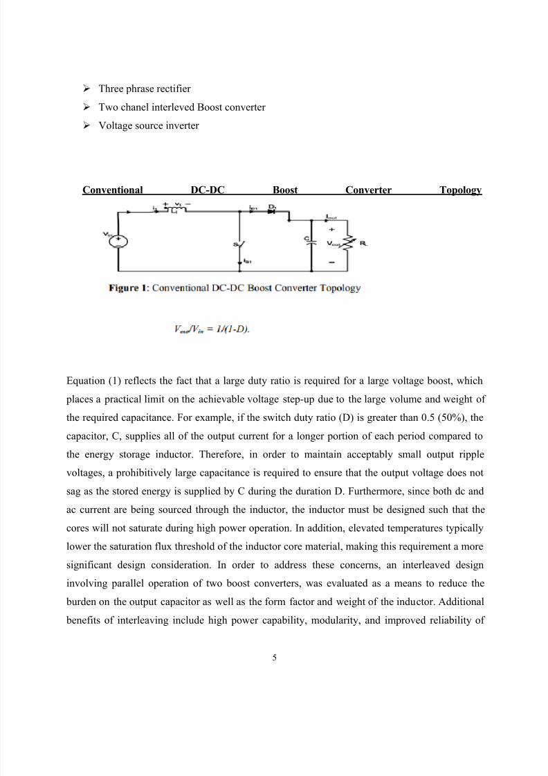
Three phrase rectifier
Two chanel interleved Boost converter
Voltage source inverter
Conventional DC-DC Boost Converter Topology
Equation (1) reflects the fact that a large duty ratio is required for a large voltage boost, which
places a practical limit on the achievable voltage step-up due to the large volume and weight of
the required capacitance. For example, if the switch duty ratio (D) is greater than 0.5 (50%), the
capacitor, C, supplies all of the output current for a longer portion of each period compared to
the energy storage inductor. Therefore, in order to maintain acceptably small output ripple
voltages, a prohibitively large capacitance is required to ensure that the output voltage does not
sag as the stored energy is supplied by C during the duration D. Furthermore, since both dc and
ac current are being sourced through the inductor, the inductor must be designed such that the
cores will not saturate during high power operation. In addition, elevated temperatures typically
lower the saturation flux threshold of the inductor core material, making this requirement a more
significant design consideration. In order to address these concerns, an interleaved design
involving parallel operation of two boost converters, was evaluated as a means to reduce the
burden on the output capacitor as well as the form factor and weight of the inductor. Additional
benefits of interleaving include high power capability, modularity, and improved reliability of
7/21/2019 Proiect SEU
http://slidepdf.com/reader/full/proiect-seu 6/34
6
the converter. An interleaved topology, however, improves converter performance at the cost of
additional inductors, power switching devices, and output rectifiers. Since the inductor is the
largest and heaviest component in a power boost converter, the use of a coupled inductor, where
a core is shared by multiple converters instead of using multiple discrete inductors, offers a
potential approach to reducing parts count, volume, and weight. Coupled inductor topologies can
also provide additional advantages such as reduced core and winding loss as well as improved
input and inductor current ripple characteristics. Properly implemented, the coupled inductor can
also yield a decrease in electromagnetic emission, an increase in efficiency, and improved
transient response. Inductor flux coupling can be realized using either direct or indirect winding
configurations and is a primary design consideration for the interleaved topology. Descriptions
of the benefits and disadvantages of each configuration are more fully described below.
A generalized steady state analysis of multiphase interleaved boost converters has been
previously reported in detail in [3]. Useful design equations for operation of an interleaved boost
converter along with the effects of inductor coupling on the key converter performance
parameters such as inductor ripple current, input ripple current, minimum load current
requirement
Differences between a single phase and a multiphase converterA multiphase converter consists of paralleled power stages, which drive a common load. By
phase shifting the PWM signals to the converter power stages, or “channels”, several advantages
over a single power stage including lower current ripple on the input and output capacitors, faster
transient response to load steps, improved power handling capabilities, and higher system
efficiency are obtained.
7/21/2019 Proiect SEU
http://slidepdf.com/reader/full/proiect-seu 7/34
7
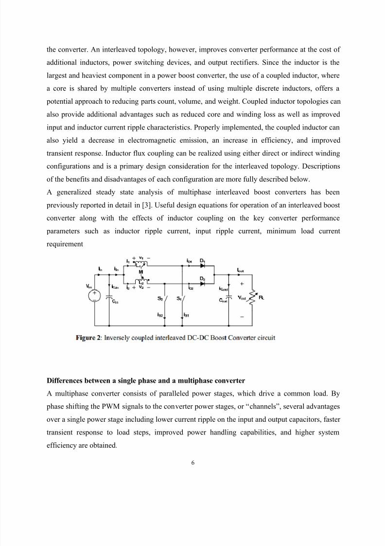
Interleaved Boost converter Operation
Fig. 2 shows the schematic of the dual interleaved boost dc-dc converter. The interleaved boost
dc-dc converter consists of two parallel connected boost converter units, which are controlled by
a phase-shifted switching function (interleaved operation). To illustrate interleaving operation,
Fig. 3 shows the timing diagram of control signals to the switches Since this converter has two
parallel units, the duty cycle for each unit is equal to (Vout-Vin)/Vout, and it is same for each
unit due to parallel configuration. A phase shift should be implemented between the timing
signals of the first and the second switch. Since there are two units parallel in this converter, the
phase shift value is 180O.
The states of operation of this converter are explained as follows. In order to simplify the
calculation, it is assumed that the inductance value of both inductor are L1 and L2, where
L1=L2=L, and the duty cycle of Q1 and Q2 denoted as D1and D2, with D1=D2=D.
1). State a:
At time t0, Q1 is closed and Q2 is opened. The current of the inductor L1 starts to rise, while L2
continues to discharge. The rate of change of iLl is diLl/dt = Vi/L, while the rate of change of
iL2 is diL2/dt = (Vi – Vo)/L.

7/21/2019 Proiect SEU
http://slidepdf.com/reader/full/proiect-seu 8/34
8
2). State b:
At time t1, Q1 and Q2 are opened. The inductors L1 and L2 discharge through the load. The rate
of change of iLl and iL2 are diLl/dt = diL2/dt = (Vi – Vo)/L.
3). State c:
At time t2, Q2 is closed while Q1 still opened. The current of the inductor L2 starts to rise, while
L1 continues to discharge. The rate of change of iL2 is diL2/dt = Vi/L, while the rate of change
of iL1 is diL1/dt = (Vi – Vo)/L.
4). State d:
At time t3, Q2 is opened and Q1 still opened. The situation is same as state b. The inductors L1
and L2 discharge
through the load. The rate of change of iLl and iL2 are diLl/dt = diL2/dt = (Vi – Vo)/L.
Due to the symmetry of the circuit, the next state is similar to the previous.
Operating principle
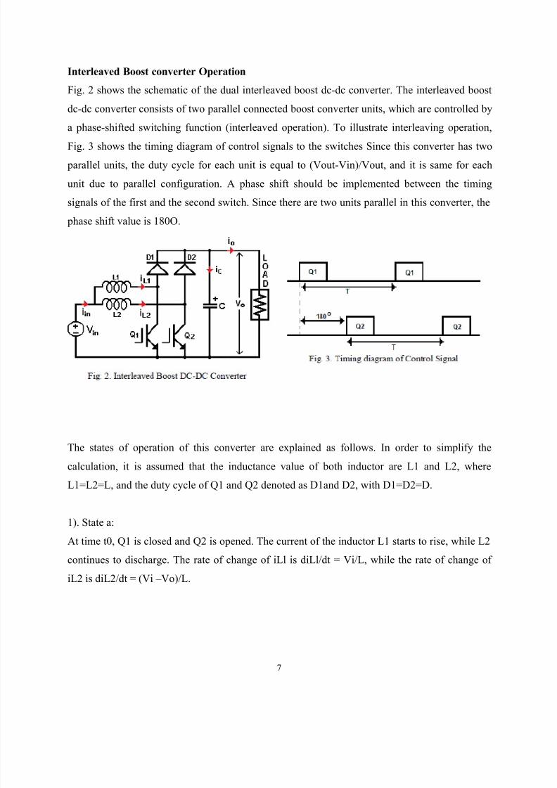
Continuous mode
When a boost converter operates in continuous mode, the current through the inductor (I_L)never falls to zero. Figure 3 shows the typical waveforms of currents and voltages in a converter
operating in this mode. The output voltage can be calculated as follows, in the case of an ideal
converter (i.e. using components with an ideal behaviour) operating in steady conditions
During the On-state, the switch S is closed, which makes the input voltage (V_i) appear across
the inductor, which causes a change in current (I_L) flowing through the inductor during a time
period (t) by the formula:
7/21/2019 Proiect SEU
http://slidepdf.com/reader/full/proiect-seu 9/34
9
D is the duty cycle. It represents the fraction of the commutation period T during which the
switch is On. Therefore D ranges between 0 (S is never on) and 1 (S is always on). During the
Off-state, the switch S is open, so the inductor current flows through the load. If we consider
zero voltage drop in the diode, and a capacitor large enough for its voltage to remain constant,
the evolution of IL is:
Waveforms of current and voltage in a boost converter operating in continuous mode.
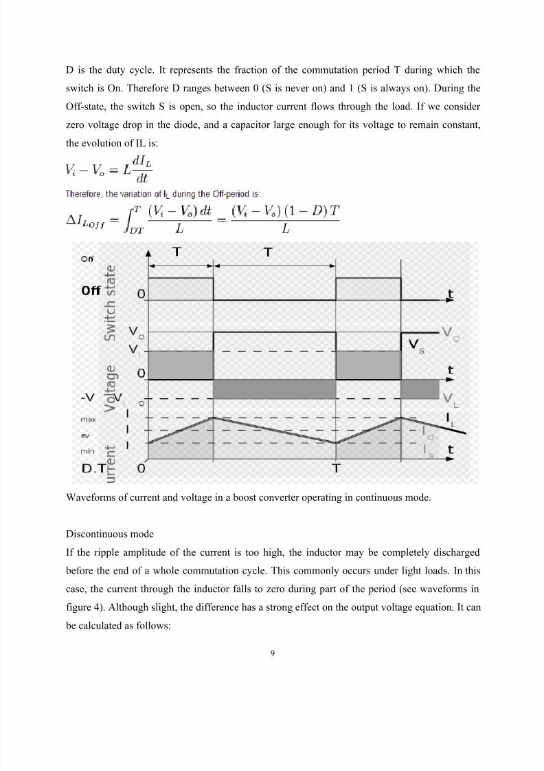
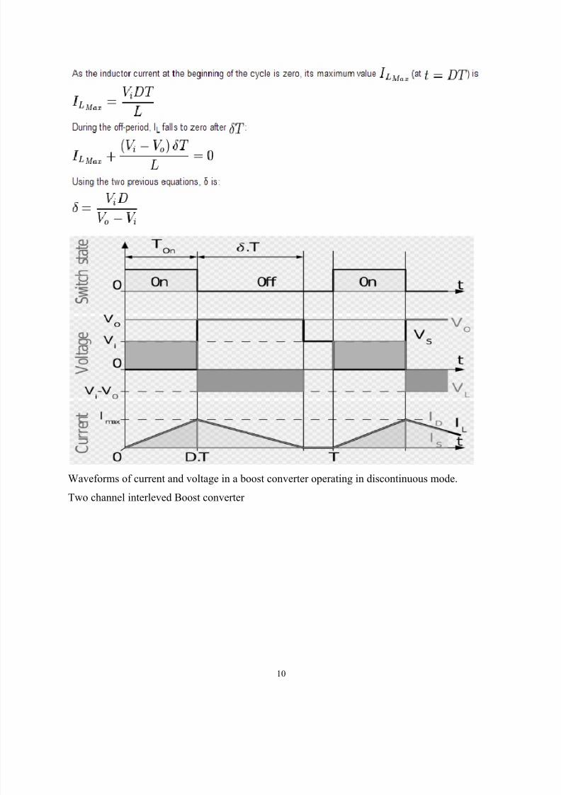
Discontinuous mode
If the ripple amplitude of the current is too high, the inductor may be completely discharged
before the end of a whole commutation cycle. This commonly occurs under light loads. In this
case, the current through the inductor falls to zero during part of the period (see waveforms in
figure 4). Although slight, the difference has a strong effect on the output voltage equation. It can
be calculated as follows:
7/21/2019 Proiect SEU
http://slidepdf.com/reader/full/proiect-seu 10/34
10
Waveforms of current and voltage in a boost converter operating in discontinuous mode.
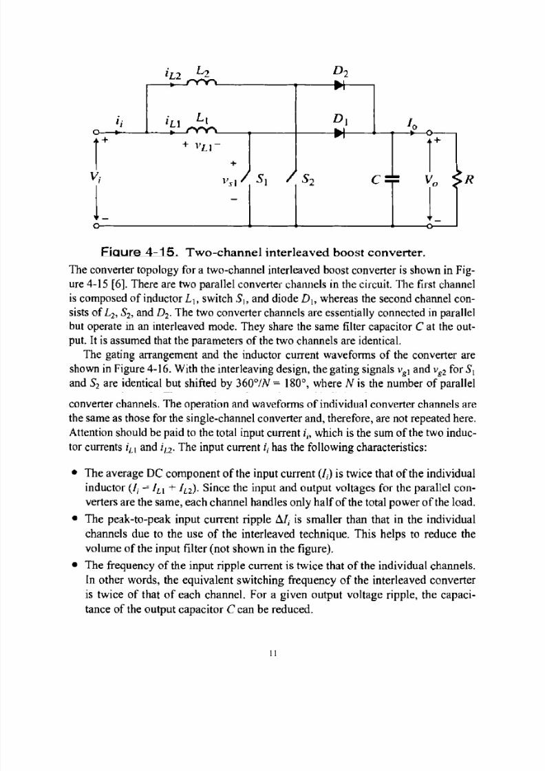
Two channel interleved Boost converter
7/21/2019 Proiect SEU
http://slidepdf.com/reader/full/proiect-seu 11/34
11
7/21/2019 Proiect SEU
http://slidepdf.com/reader/full/proiect-seu 12/34
12
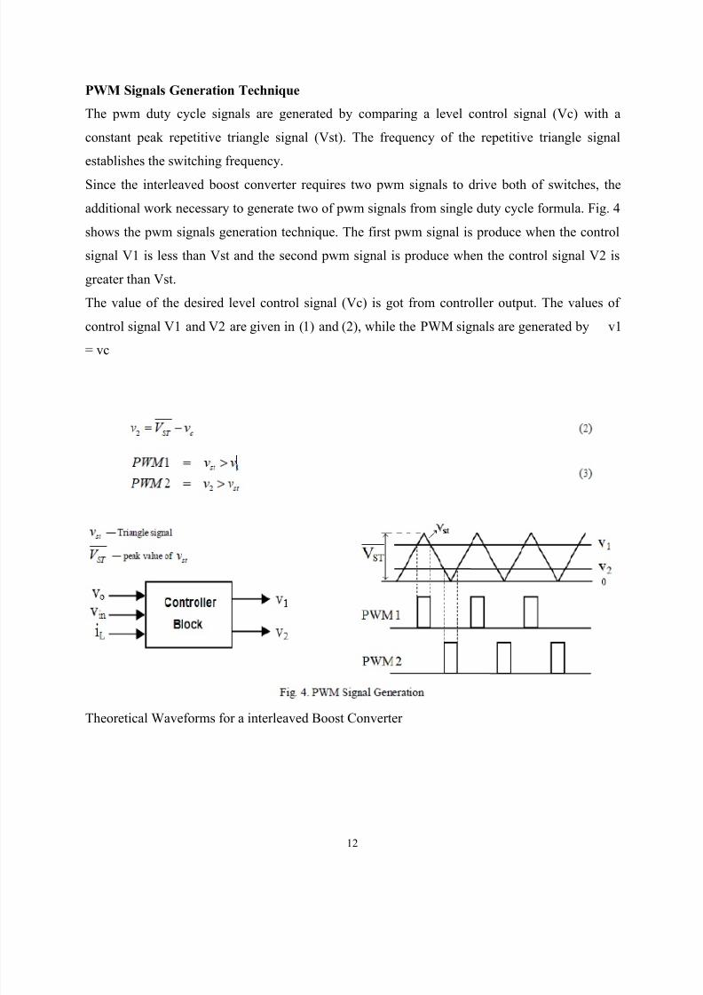
PWM Signals Generation Technique
The pwm duty cycle signals are generated by comparing a level control signal (Vc) with a
constant peak repetitive triangle signal (Vst). The frequency of the repetitive triangle signal
establishes the switching frequency.
Since the interleaved boost converter requires two pwm signals to drive both of switches, the
additional work necessary to generate two of pwm signals from single duty cycle formula. Fig. 4
shows the pwm signals generation technique. The first pwm signal is produce when the control
signal V1 is less than Vst and the second pwm signal is produce when the control signal V2 is
greater than Vst.
The value of the desired level control signal (Vc) is got from controller output. The values of
control signal V1 and V2 are given in (1) and (2), while the PWM signals are generated by v1
= vc
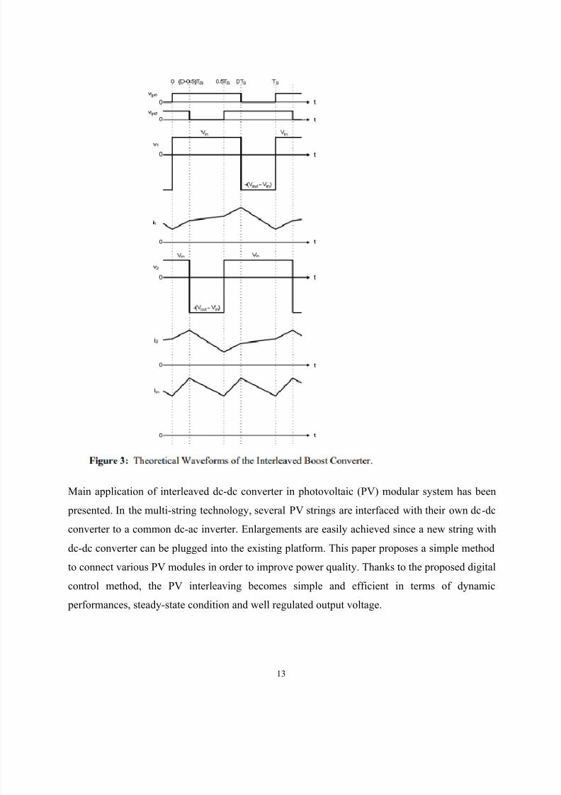
Theoretical Waveforms for a interleaved Boost Converter
7/21/2019 Proiect SEU
http://slidepdf.com/reader/full/proiect-seu 13/34
13
Main application of interleaved dc-dc converter in photovoltaic (PV) modular system has been
presented. In the multi-string technology, several PV strings are interfaced with their own dc-dc
converter to a common dc-ac inverter. Enlargements are easily achieved since a new string with
dc-dc converter can be plugged into the existing platform. This paper proposes a simple method
to connect various PV modules in order to improve power quality. Thanks to the proposed digital
control method, the PV interleaving becomes simple and efficient in terms of dynamic
performances, steady-state condition and well regulated output voltage.
7/21/2019 Proiect SEU
http://slidepdf.com/reader/full/proiect-seu 14/34
14
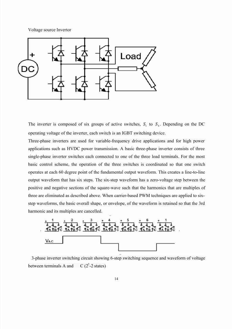
Voltage source Invertor
The inverter is composed of six groups of active switches,1
S to6
S . Depending on the DC
operating voltage of the inverter, each switch is an IGBT switching device.
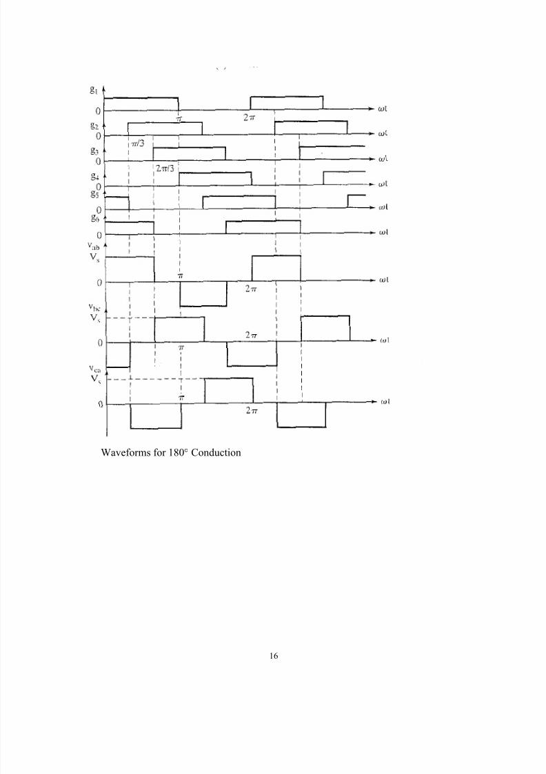
Three-phase inverters are used for variable-frequency drive applications and for high power
applications such as HVDC power transmission. A basic three-phase inverter consists of three
single-phase inverter switches each connected to one of the three load terminals. For the most
basic control scheme, the operation of the three switches is coordinated so that one switch
operates at each 60 degree point of the fundamental output waveform. This creates a line-to-line
output waveform that has six steps. The six-step waveform has a zero-voltage step between the
positive and negative sections of the square-wave such that the harmonics that are multiples of
three are eliminated as described above. When carrier-based PWM techniques are applied to six-
step waveforms, the basic overall shape, or envelope, of the waveform is retained so that the 3rd
harmonic and its multiples are cancelled.
3-phase inverter switching circuit showing 6-step switching sequence and waveform of voltage
between terminals A and C (23-2 states)
7/21/2019 Proiect SEU
http://slidepdf.com/reader/full/proiect-seu 15/34
15
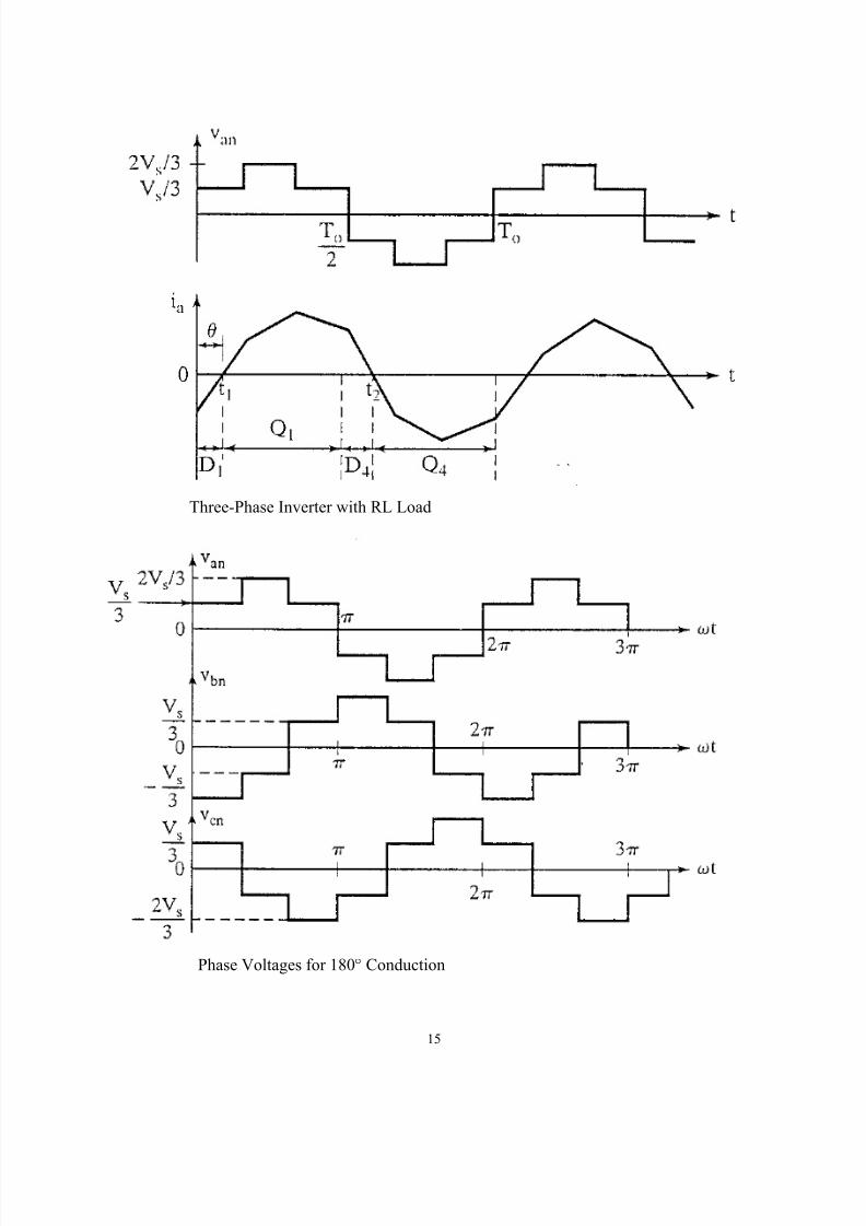
Three-Phase Inverter with RL Load
Phase Voltages for 180 Conduction
7/21/2019 Proiect SEU
http://slidepdf.com/reader/full/proiect-seu 16/34
16
Waveforms for 180 Conduction

7/21/2019 Proiect SEU
http://slidepdf.com/reader/full/proiect-seu 17/34
17
Inverter switching states
Stage I of the inverter:
Stage II of the inverter:
cba
Z
U I I Z Z
I Z I U
d
d
3
2
2
3
2
d ad
d
a U uU Z
Z
U Z I u
3
2
3
2
3
2
d bd
d
d
b U uU Z
Z
U Z
U
Z I
u3
1
3
1
2
1
3
2
2
3
2
2
d cd
d
d
c U uU Z
Z
U Z
U
Z I
u3
1
3
1
2
1
3
2
2
3
2
2
Z
U I I Z Z I Z
I U
d
d
3
2
2
3
2
d ad
d
d
a U uU
Z
U Z
Z
U
Z I
Z u3
1
3
1
2
1
3
2
2
2
3
2

7/21/2019 Proiect SEU
http://slidepdf.com/reader/full/proiect-seu 18/34
18
Stage III of the inverter:
d bd
d
d
b U uU
Z
U Z
Z
U
Z I
Z u3
1
3
1
2
1
3
2
2
2
3
2
d cd
d
c U uU
Z
U Z Z I u
3
2
3
2
3
2
Z
U I I Z
I Z I Z U
d
d
3
2
2
3
2
d ad
d
d
a U uU
Z
U Z
U
Z I
Z u3
1
3
1
2
1
3
2
2
3
2
2
d bd
d
b U uU
Z
Z
U
Z I Z u3
2
3
2
d cd
d
d
c U uU Z Z
U Z
U
Z I
Z u3
1
3
1
2
1
3
2
2
3
2
2

7/21/2019 Proiect SEU
http://slidepdf.com/reader/full/proiect-seu 19/34
19
Stage IV of the inverter:
Stage V of the inverter:
Z
U I
I Z Z I Z
I U
d
d
3
2
2
3
2
d ad
d
a U uU Z
Z
U Z I u
3
2
3
2
3
2
d bd
d
d
b U uU
Z
U Z
Z
U
Z I
Z u3
1
3
1
2
1
3
2
2
3
2
2
d cd
d
d
c U uU
Z
U Z
Z
U
Z I
Z u3
1
3
1
2
1
3
2
2
3
2
2
Z
U I I Z Z
I Z I U
d
d
3
2
2
3
2
d ad
d
d
a U uU
Z
U Z
Z
U
Z I
Z u3
1
3
1
2
1
3
2
2
3
2
2
d bd
d
d
b U uU
Z
U Z
Z
U
Z I
Z u3
1
3
1
2
1
3
2
2
3
2
2

7/21/2019 Proiect SEU
http://slidepdf.com/reader/full/proiect-seu 20/34
20
Stage VI of the inverter:
d cd
d
c U uU
Z
U Z Z I u
3
2
3
2
3
2
Z
U I I Z Z I Z
I U
d
d
3
2
2
3
2
d ad
d
d
a U uU
Z
U Z
Z
U
Z I
Z u3
1
3
1
2
1
3
2
2
2
3
2
d bd
d
b U uU
Z
U Z I Z u
3
2
3
2
3
2
d cd
d
d
c U uU
Z
U Z
Z
U
Z I
Z u3
1
3
1
2
1
3
2
2
2
3
2
7/21/2019 Proiect SEU
http://slidepdf.com/reader/full/proiect-seu 21/34
21
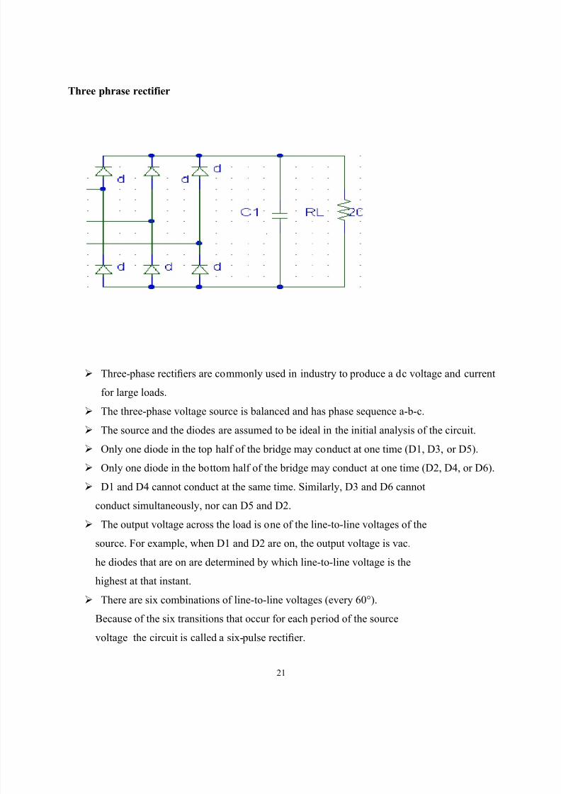
Three phrase rectifier
Three- phase rectifiers are commonly used in industry to produce a dc voltage and current
for large loads.
The three-phase voltage source is balanced and has phase sequence a-b-c.
The source and the diodes are assumed to be ideal in the initial analysis of the circuit.
Only one diode in the top half of the bridge may conduct at one time (D1, D3, or D5).
Only one diode in the bottom half of the bridge may conduct at one time (D2, D4, or D6).
D1 and D4 cannot conduct at the same time. Similarly, D3 and D6 cannot
conduct simultaneously, nor can D5 and D2.
The output voltage across the load is one of the line-to-line voltages of the
source. For example, when D1 and D2 are on, the output voltage is vac.
he diodes that are on are determined by which line-to-line voltage is the
highest at that instant.
There are six combinations of line-to-line voltages (every 60°).
Because of the six transitions that occur for each period of the source
voltage the circuit is called a six- pulse rectifier.
7/21/2019 Proiect SEU
http://slidepdf.com/reader/full/proiect-seu 22/34
22
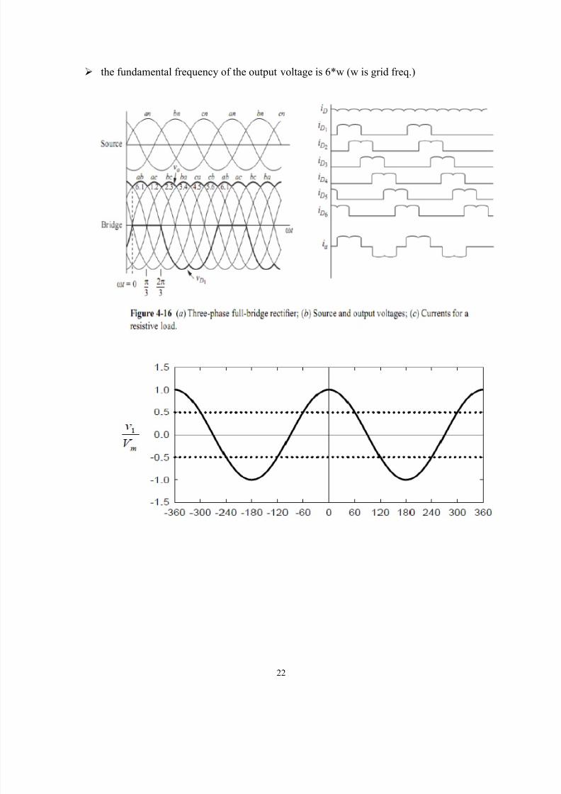
the fundamental frequency of the output voltage is 6*w (w is grid freq.)
7/21/2019 Proiect SEU
http://slidepdf.com/reader/full/proiect-seu 23/34
23
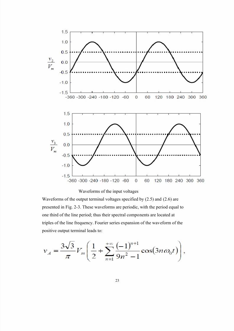
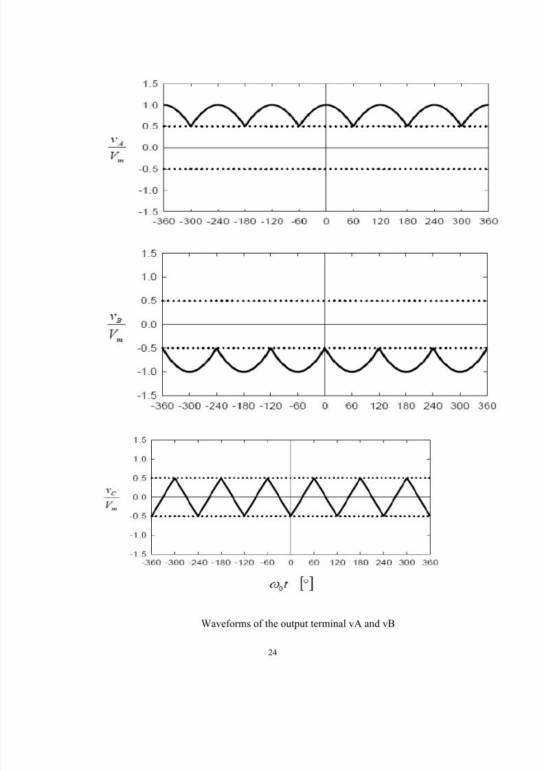
Waveforms of the input voltages
Waveforms of the output terminal voltages specified by (2.5) and (2.6) are
presented in Fig. 2-3. These waveforms are periodic, with the period equal to
one third of the line period; thus their spectral components are located at
triples of the line frequency. Fourier series expansion of the waveform of the
positive output terminal leads to:
7/21/2019 Proiect SEU
http://slidepdf.com/reader/full/proiect-seu 24/34
24
Waveforms of the output terminal vA and vB

7/21/2019 Proiect SEU
http://slidepdf.com/reader/full/proiect-seu 25/34
25
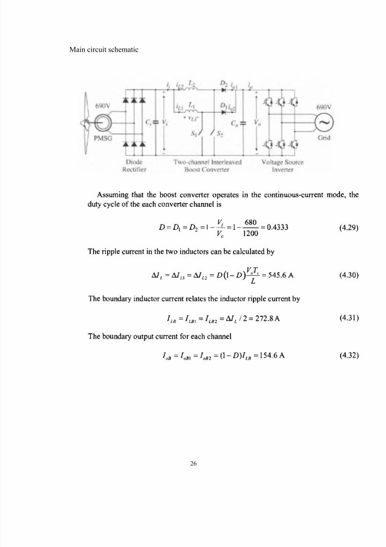
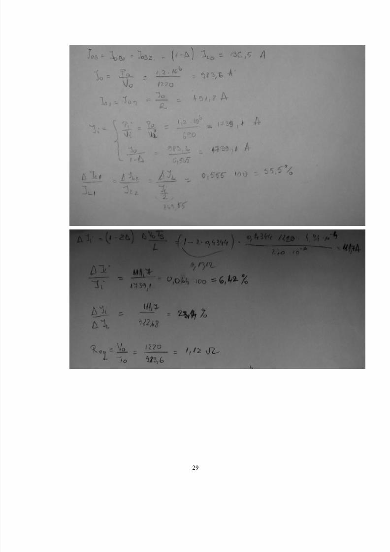
Tehnical calculations
Requirements
A two-channel boost converter is used in a 1.2 MW, 690 V, 50 Hz PMSG wind energy
conversion system as shown below. The boost converter transfers the power from the
generator to the grid of 690 V/50 Hz via a diode rectifier and a two-level voltage source
inverter. The inductance L1(L 2 = L 1 ) and capacitance Co of the boost converter are
270 µH and 2300 µF, respectively. The switching frequency of the boost converter is
2000 Hz. The output voltage Vo of the boost converter is set by the inverter to 1220 V.
At a given wind speed, the generator is delivering the rated power to the grid and its line-
to-line stator voltage is found to be 690 V. Calculate/answer the following:
a) The input voltage and power to the boost converter
b) The boundary inductor and output currents for each channel, operating mode, and
duty cycle.
c) The peak-to-peak and average inductor currents in each channel.
d) The peak-to-peak and average input currents.
e) The percentage inductor and input current ripples.
f) The percentage output voltage ripple if the boost converters are interleaved and not
interleaved.
g) Simulate the circuit using Simulink
7/21/2019 Proiect SEU
http://slidepdf.com/reader/full/proiect-seu 26/34
26
Main circuit schematic
7/21/2019 Proiect SEU
http://slidepdf.com/reader/full/proiect-seu 27/34
27

7/21/2019 Proiect SEU
http://slidepdf.com/reader/full/proiect-seu 28/34
28
Tehnical calculations acording our parameters are in the pdf file atached
7/21/2019 Proiect SEU
http://slidepdf.com/reader/full/proiect-seu 29/34
29

7/21/2019 Proiect SEU
http://slidepdf.com/reader/full/proiect-seu 30/34
30
7/21/2019 Proiect SEU
http://slidepdf.com/reader/full/proiect-seu 31/34
31
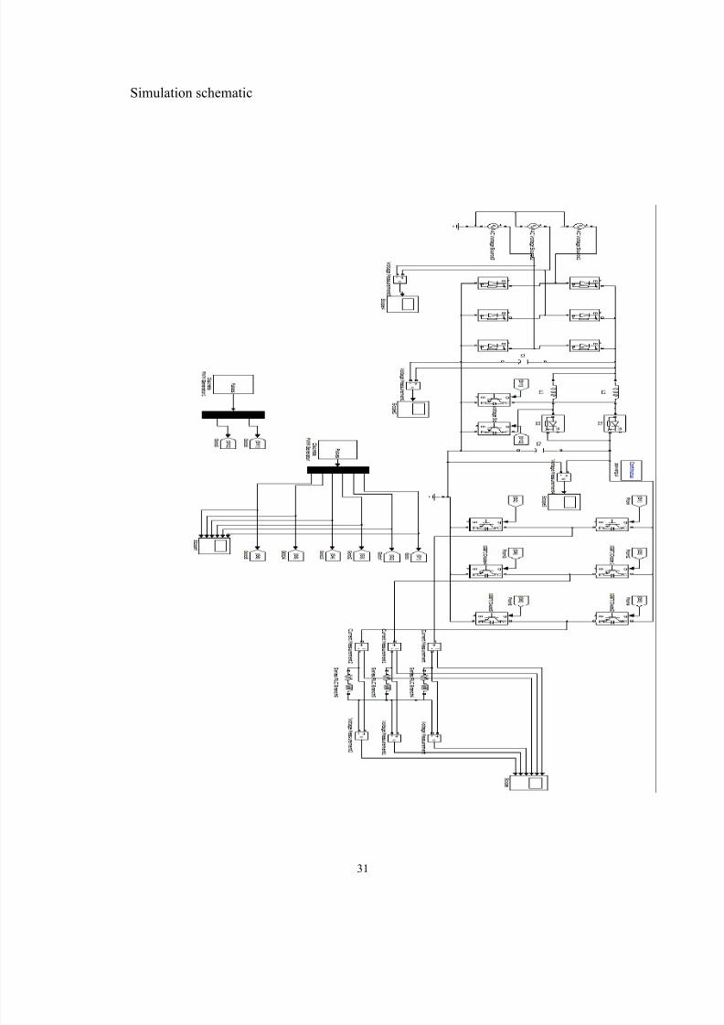
Simulation schematic
7/21/2019 Proiect SEU
http://slidepdf.com/reader/full/proiect-seu 32/34
32
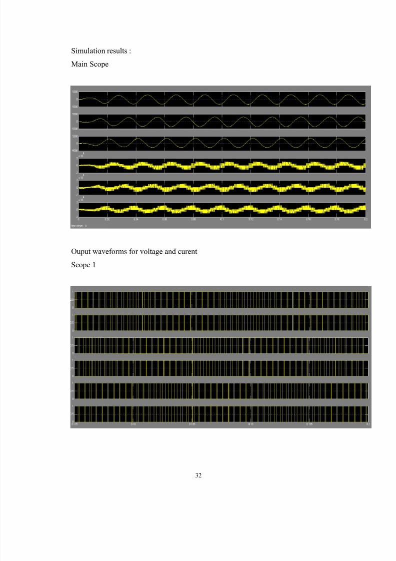
Simulation results :
Main Scope
Ouput waveforms for voltage and curent
Scope 1
7/21/2019 Proiect SEU
http://slidepdf.com/reader/full/proiect-seu 33/34
33
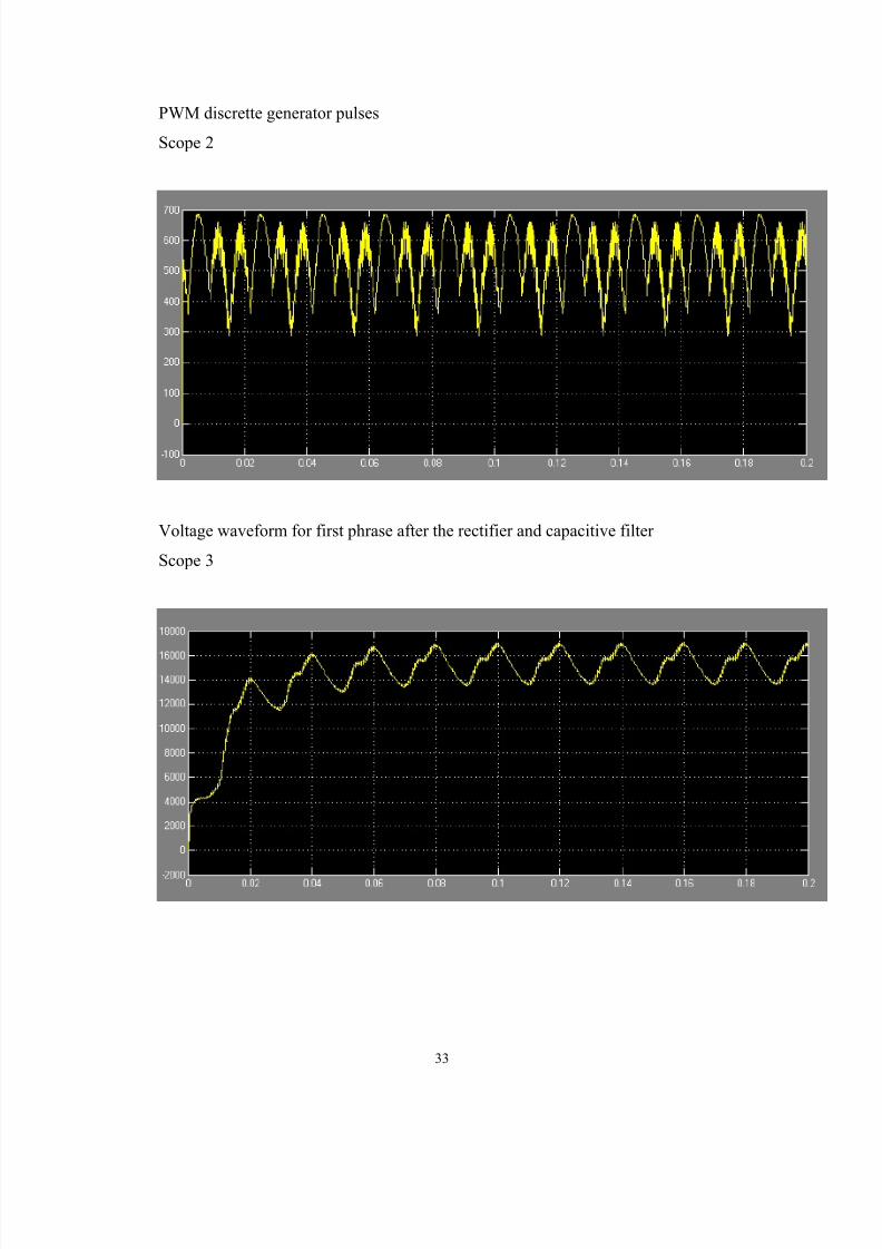
PWM discrette generator pulses
Scope 2
Voltage waveform for first phrase after the rectifier and capacitive filter
Scope 3
7/21/2019 Proiect SEU
http://slidepdf.com/reader/full/proiect-seu 34/34
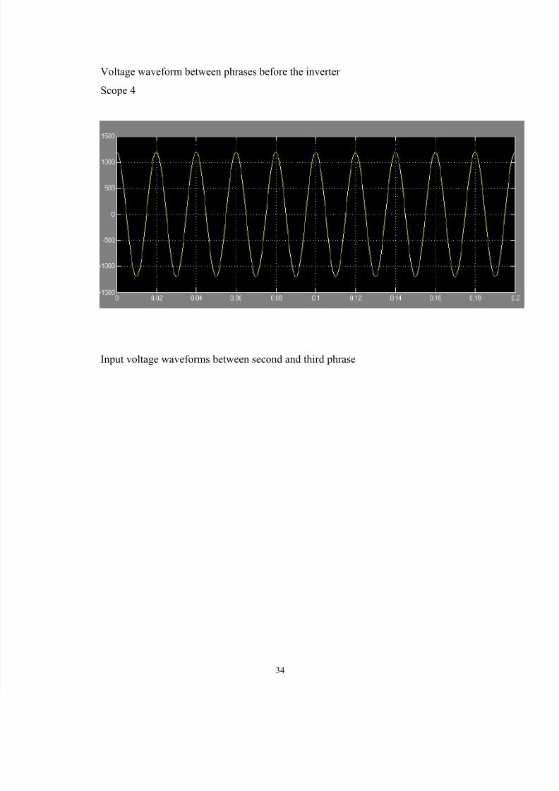
Voltage waveform between phrases before the inverter
Scope 4
Input voltage waveforms between second and third phrase


![Pif. Paf. Puf - Cezar Petrescu - cdn4.libris.ro. Paf. Puf - Cezar Petrescu.pdf · rcIU nU IUnf zeq ep ?u{d rS plrlernru giered o g 'esrusnJJ-seu euneaplolul]uns J?d rnl elrapl iml](https://static.fdocumente.com/doc/165x107/5e0b6ebd23b9300cd9458171/pif-paf-puf-cezar-petrescu-cdn4-paf-puf-cezar-petrescupdf-rciu-nu.jpg)