Tehnici nanolitografice pentru fabricarea dispozitivelor ... · Tehnici nanolitografice pentru...
22
12 October 2012 Tehnici nanolitografice pentru fabricarea dispozitivelor nanoelectronice Adrian Dinescu, IMT Bucuresti Workshop “Parteneriat pentru inovare: cercetare – industria electronica”
Transcript of Tehnici nanolitografice pentru fabricarea dispozitivelor ... · Tehnici nanolitografice pentru...
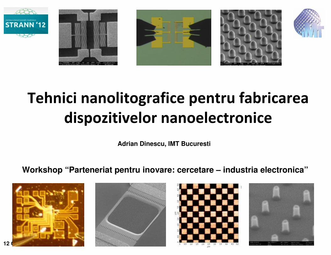
12 October 2012
Tehnici nanolitografice pentru fabricarea
dispozitivelor nanoelectronice
Adrian Dinescu, IMT Bucuresti
Workshop “Parteneriat pentru inovare: cercetare – industria electronica”
18 October 2012
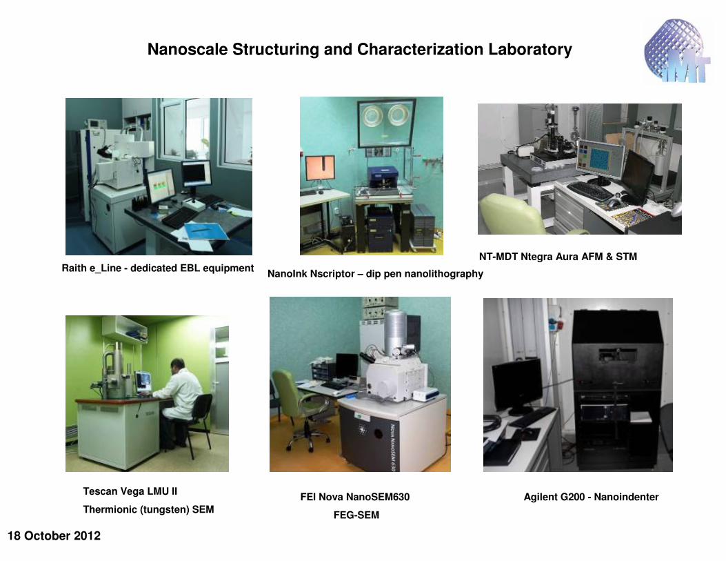
Nanoscale Structuring and Characterization Laboratory
Raith e_Line - dedicated EBL equipmentNanoInk Nscriptor – dip pen nanolithography
NT-MDT Ntegra Aura AFM & STM
Tescan Vega LMU II
Thermionic (tungsten) SEM
FEI Nova NanoSEM630
FEG-SEM
Agilent G200 - Nanoindenter
18 October 2012
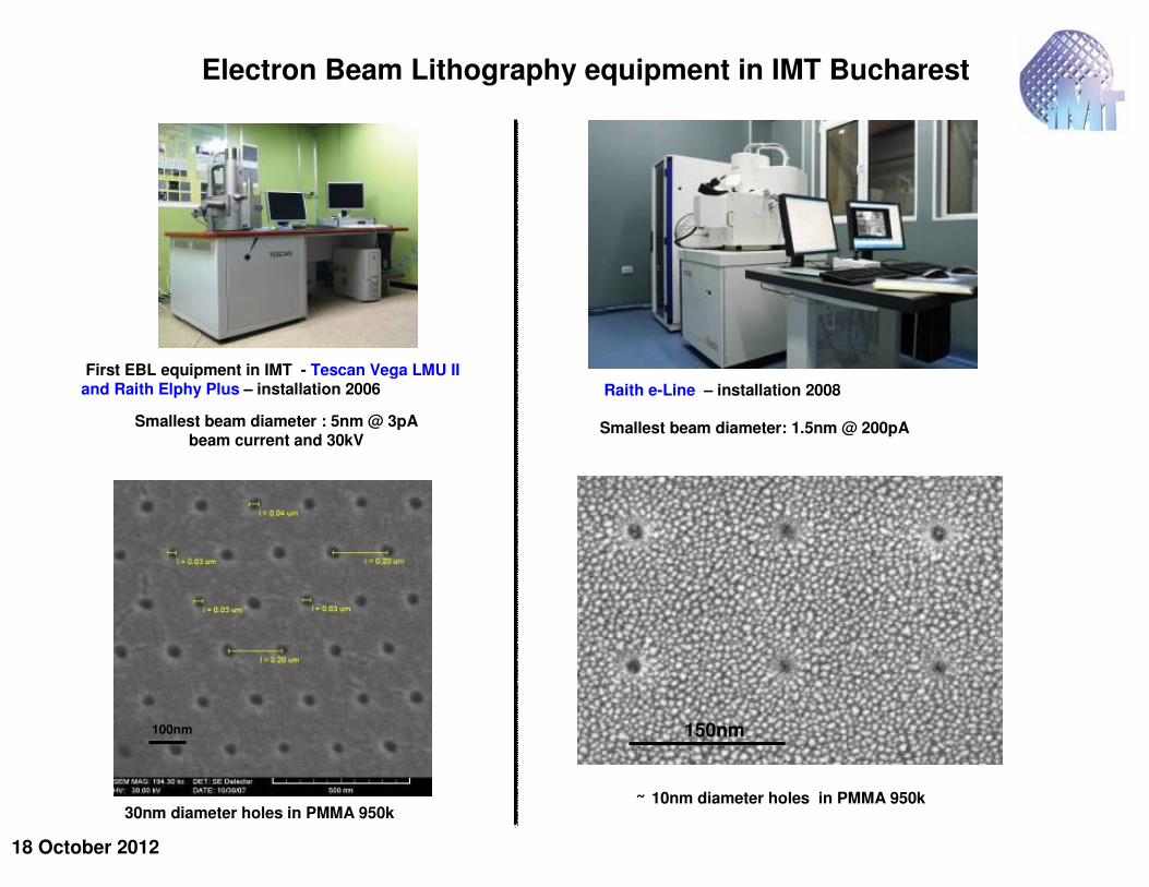
First EBL equipment in IMT - Tescan Vega LMU II and Raith Elphy Plus – installation 2006 Raith e-Line – installation 2008
150nm
30nm diameter holes in PMMA 950k 10nm diameter holes in PMMA 950k
Smallest beam diameter : 5nm @ 3pA beam current and 30kV
Smallest beam diameter: 1.5nm @ 200pA
Electron Beam Lithography equipment in IMT Bucharest
100nm
18 October 2012
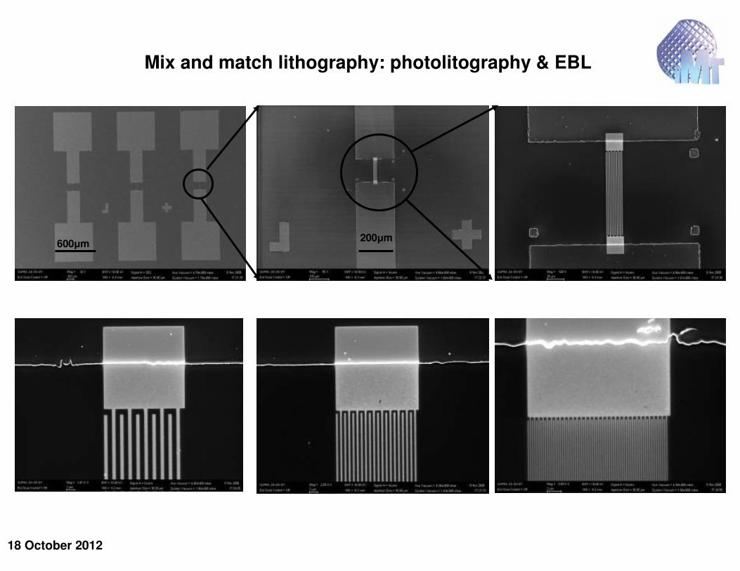
Mix and match lithography: photolitography & EBL
600µm200µm
18 October 2012
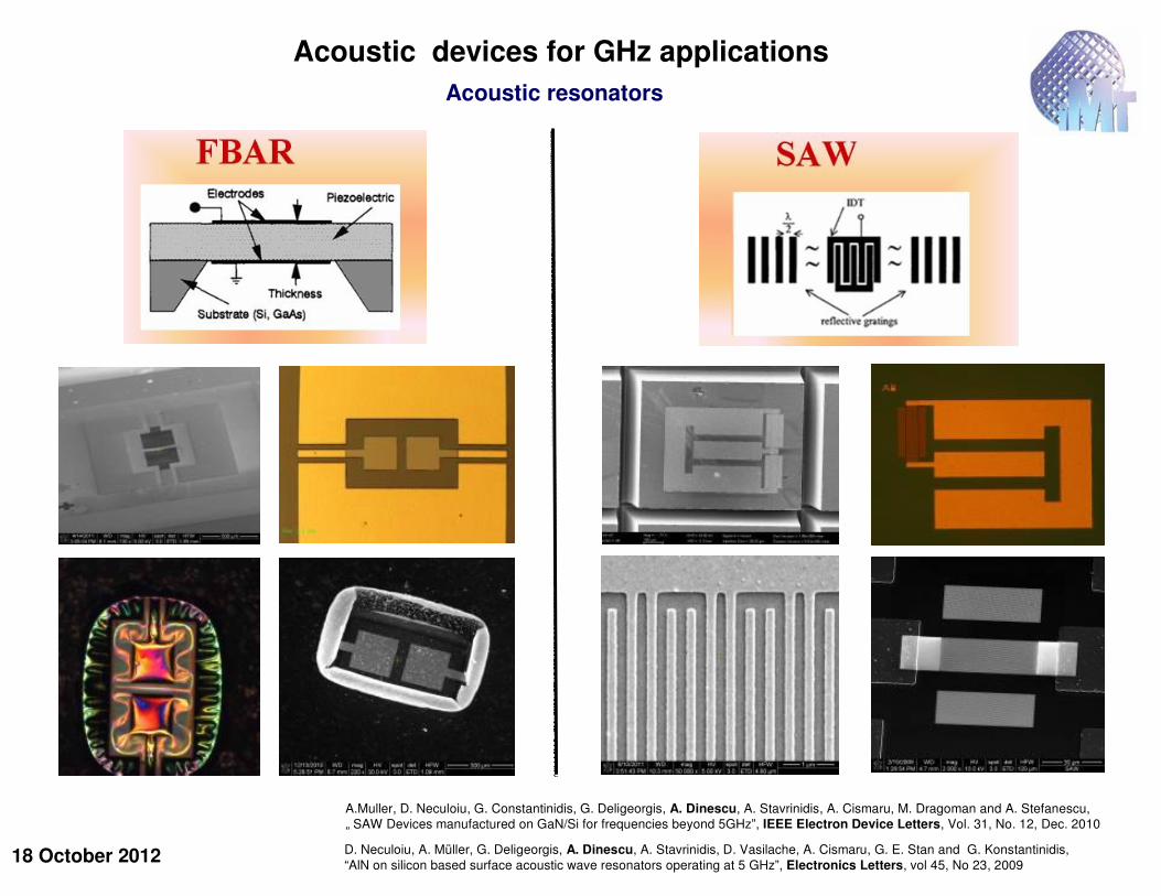
Acoustic devices for GHz applications
Acoustic resonators
A.Muller, D. Neculoiu, G. Constantinidis, G. Deligeorgis, A. Dinescu, A. Stavrinidis, A. Cismaru, M. Dragoman and A. Stefanescu,
„ SAW Devices manufactured on GaN/Si for frequencies beyond 5GHz”, IEEE Electron Device Letters, Vol. 31, No. 12, Dec. 2010
D. Neculoiu, A. Müller, G. Deligeorgis, A. Dinescu, A. Stavrinidis, D. Vasilache, A. Cismaru, G. E. Stan and G. Konstantinidis,
“AlN on silicon based surface acoustic wave resonators operating at 5 GHz”, Electronics Letters, vol 45, No 23, 2009
18 October 2012
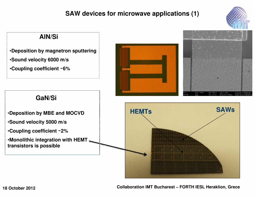
SAW devices for microwave applications (1)
AlN/Si
•Deposition by magnetron sputtering
•Sound velocity 6000 m/s
•Coupling coefficient 6%
•Deposition by MBE and MOCVD
•Sound velocity 5000 m/s
•Coupling coefficient 2%
•Monolithic integration with HEMT transistors is possible
SAWsHEMTs
GaN/Si
Collaboration IMT Bucharest – FORTH IESL Heraklion, Grece
18 October 2012
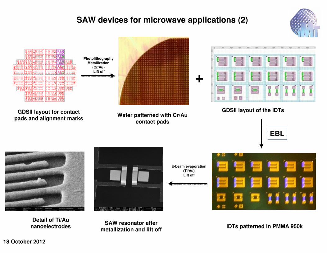
SAW devices for microwave applications (2)
GDSII layout for contact pads and alignment marks
Wafer patterned with Cr/Au contact pads
GDSII layout of the IDTs
IDTs patterned in PMMA 950kSAW resonator after
metallization and lift off
Detail of Ti/Au nanoelectrodes
Photolithography Metallization
(Cr/Au)Lift off
+
EBL
E-beam evaporation (Ti/Au)
Lift off
18 October 2012
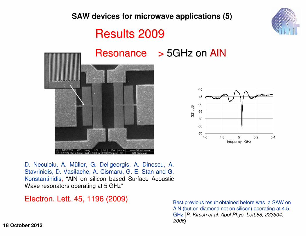
D. Neculoiu, A. Müller, G. Deligeorgis, A. Dinescu, A. Stavrinidis, D. Vasilache, A. Cismaru, G. E. Stan and G.
Konstantinidis, “AlN on silicon based Surface Acoustic Wave resonators operating at 5 GHz”
Electron. Lett. 45, 1196 (2009)Electron. Lett. 45, 1196 (2009)Best previous result obtained before was a SAW on
AlN (but on diamond not on silicon) operating at 4.5
GHz [P. Kirsch et al. Appl Phys. Lett.88, 223504,
2006]
4.6 4.8 5 5.2 5.4
frequency, GHz
-70
-65
-60
-55
-50
-45
-40
S21, dB
Results 2009Results 2009
Resonance > Resonance > 5GHz on 5GHz on AlNAlN
SAW devices for microwave applications (5)
18 October 2012
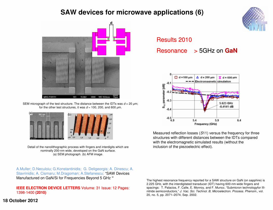
SAW devices for microwave applications (6)
Results 2010 Results 2010
Resonance > Resonance > 5GHz on 5GHz on GaNGaN
The highest resonance frequency reported for a SAW structure on GaN (on sapphire) is
2.225 GHz, with the interdigitated transducer (IDT) having 600-nm-wide fingers and
spacings: T. Palacios, F. Calle, E. Monroy, and F. Munoz, “Submicron technologyfor III-
nitride semiconductors,” J. Vac. Sci. Technol. B, Microelectron. Process. Phenom., vol.
20, no. 5, pp. 2071–2074, Sep. 2002.
A.Muller; D.Neculoiu; G.Konstantinidis; G. Deligeorgis; A. Dinescu; A. Stavrinidis; A. Cismaru; M.Dragoman; A.Stefanescu; “SAW Devices Manufactured on GaN/Si for Frequencies Beyond 5 GHz “
IEEE ELECTRON DEVICE LETTERS IEEE ELECTRON DEVICE LETTERS Volume: 31 Issue: 12 Pages: Volume: 31 Issue: 12 Pages:
13981398--1400 1400 (2010)(2010)
SEM micrograph of the test structure. The distance between the IDTs was d = 20 µm;
for the other test structures, it was d = 100, 200, and 600 µm.
Measured reflection losses (S11) versus the frequency for threestructures with different distances between the IDTs compared with the electromagnetic simulated results (without the inclusion of the piezoelectric effect).Detail of the nanolithographic process with fingers and interdigits which are
nominally 200-nm wide, developed on the GaN surface.
(a) SEM photograph. (b) AFM image.
18 October 2012
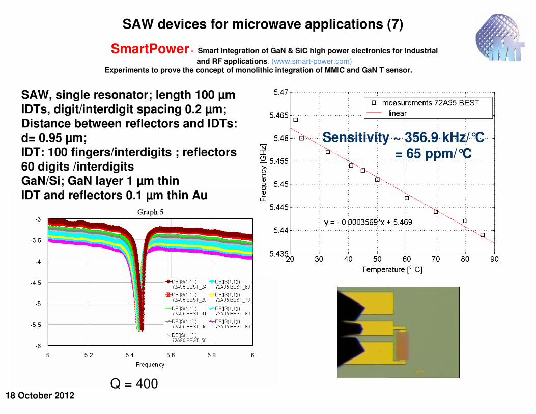
SAW, single resonator; length 100 µm IDTs, digit/interdigit spacing 0.2 µm; Distance between reflectors and IDTs: d= 0.95 µm;IDT: 100 fingers/interdigits ; reflectors 60 digits /interdigitsGaN/Si; GaN layer 1 µm thinIDT and reflectors 0.1 µm thin Au
Sensitivity ~ 356.9 kHz/°C = 65 ppm/°C
Q = 400
SAW devices for microwave applications (7)
SmartPower - Smart integration of GaN & SiC high power electronics for industrial
and RF applications. (www.smart-power.com)Experiments to prove the concept of monolithic integration of MMIC and GaN T sensor.
18 October 2012
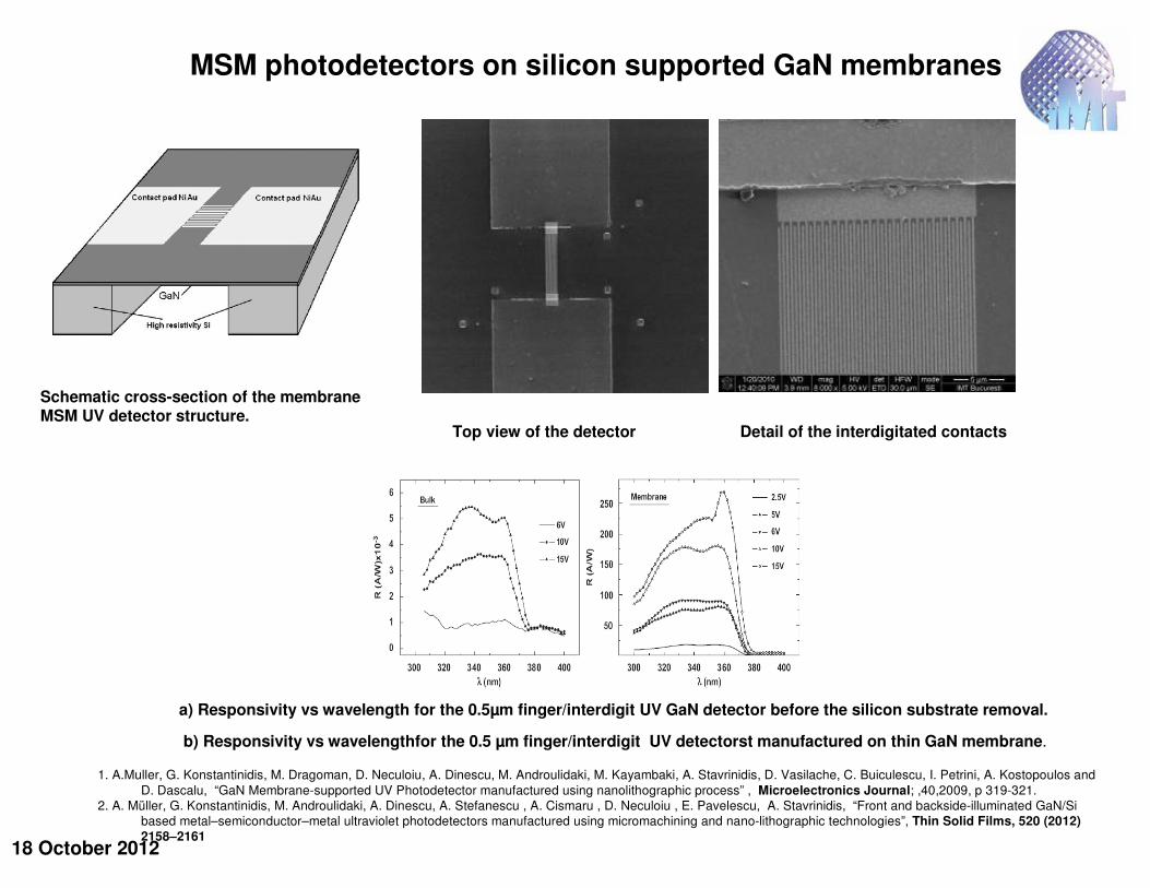
1. A.Muller, G. Konstantinidis, M. Dragoman, D. Neculoiu, A. Dinescu, M. Androulidaki, M. Kayambaki, A. Stavrinidis, D. Vasilache, C. Buiculescu, I. Petrini, A. Kostopoulos and
D. Dascalu, “GaN Membrane-supported UV Photodetector manufactured using nanolithographic process” , Microelectronics Journal; ,40,2009, p 319-321.
2. A. Müller, G. Konstantinidis, M. Androulidaki, A. Dinescu, A. Stefanescu , A. Cismaru , D. Neculoiu , E. Pavelescu, A. Stavrinidis, “Front and backside-illuminated GaN/Si
based metal–semiconductor–metal ultraviolet photodetectors manufactured using micromachining and nano-lithographic technologies”, Thin Solid Films, 520 (2012) 2158–2161
Schematic cross-section of the membrane MSM UV detector structure.
Top view of the detector Detail of the interdigitated contacts
a) Responsivity vs wavelength for the 0.5µm finger/interdigit UV GaN detector before the silicon substrate removal.
b) Responsivity vs wavelengthfor the 0.5 µm finger/interdigit UV detectorst manufactured on thin GaN membrane.
MSM photodetectors on silicon supported GaN membranes
18 October 2012
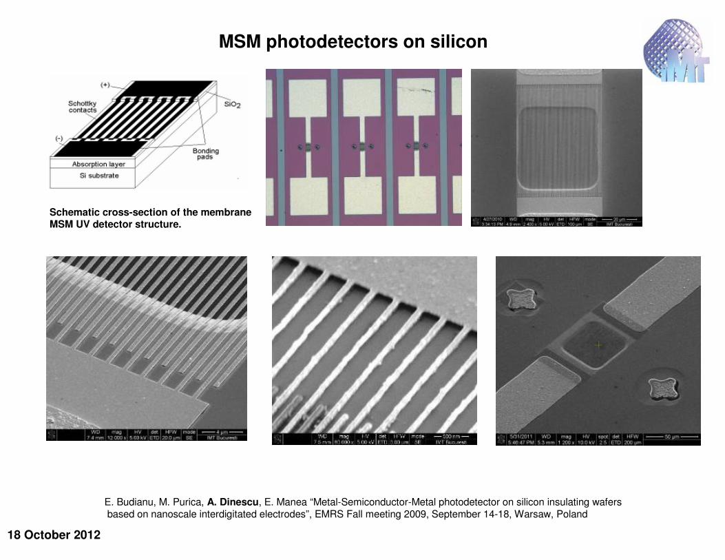
E. Budianu, M. Purica, A. Dinescu, E. Manea “Metal-Semiconductor-Metal photodetector on silicon insulating wafersbased on nanoscale interdigitated electrodes”, EMRS Fall meeting 2009, September 14-18, Warsaw, Poland
Schematic cross-section of the membrane MSM UV detector structure.
MSM photodetectors on silicon
18 October 2012
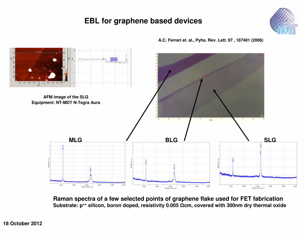
EBL for graphene based devices
Inte
nsi
ty (
a. u.)
1 500 2 000 2 500 3 000 3 500 4 000Raman shift (cm-1)
26
40
.7
15
86
.1
Inte
nsi
ty (
a. u.)
1 500 2 000 2 500 3 000 3 500 4 000Raman shift (cm-1)
26
57
.6 15
83
.2
Inte
nsi
ty (
a. u
.)
1 500 2 000 2 500 3 000 3 500 4 000Raman shift (cm-1)
2656.7
1581.0
Raman spectra of a few selected points of graphene flake used for FET fabricationSubstrate: p++ silicon, boron doped, resistivity 0.005 Ωcm, covered with 300nm dry thermal oxide
MLG BLG SLG
AFM image of the SLG
Equipment: NT-MDT N-Tegra Aura
A.C. Ferrari et. al., Pyhs. Rev. Lett. 97 , 187401 (2006)
18 October 2012
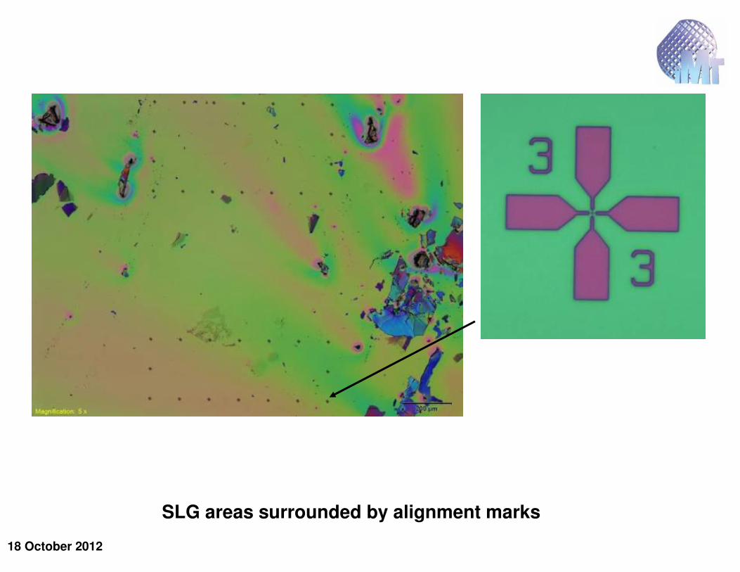
SLG areas surrounded by alignment marks
18 October 2012
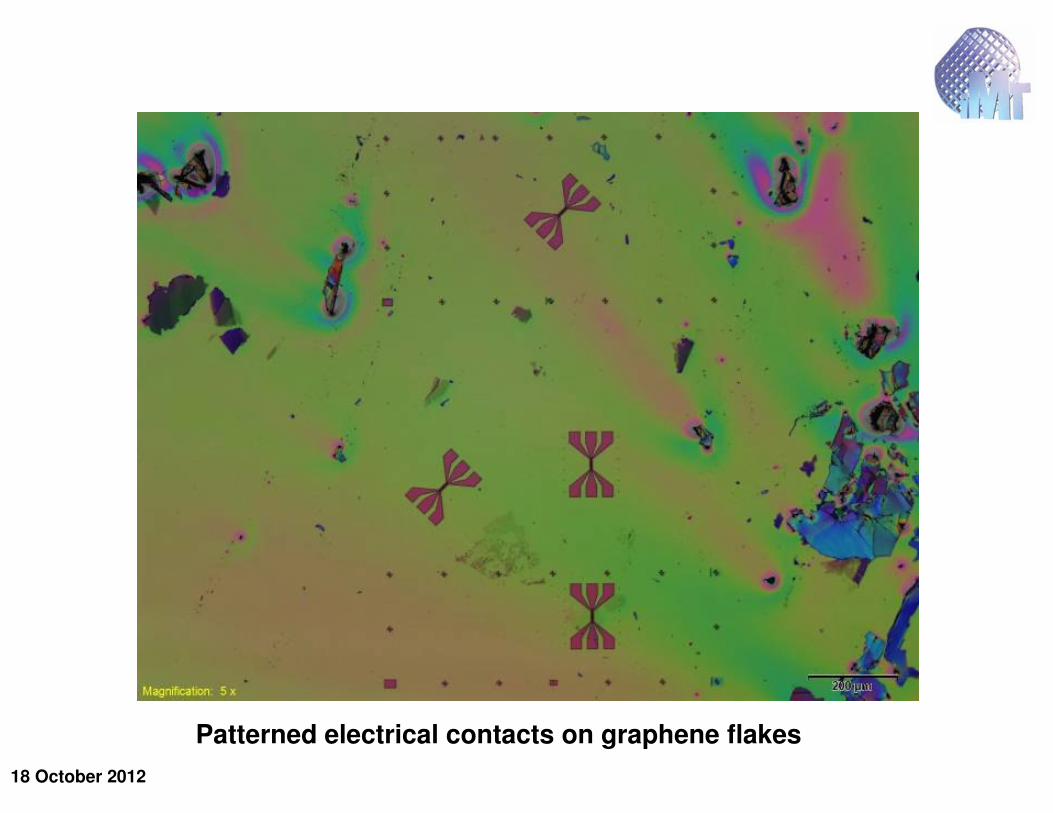
Patterned electrical contacts on graphene flakes
18 October 2012
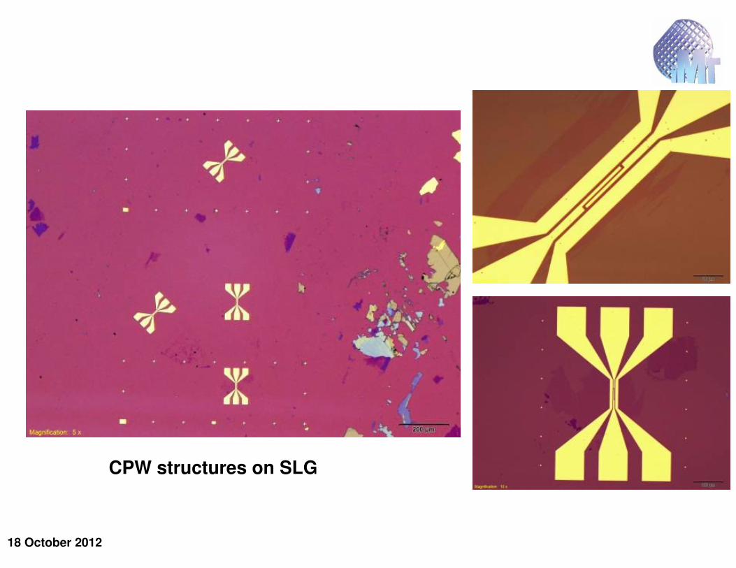
CPW structures on SLG
18 October 2012
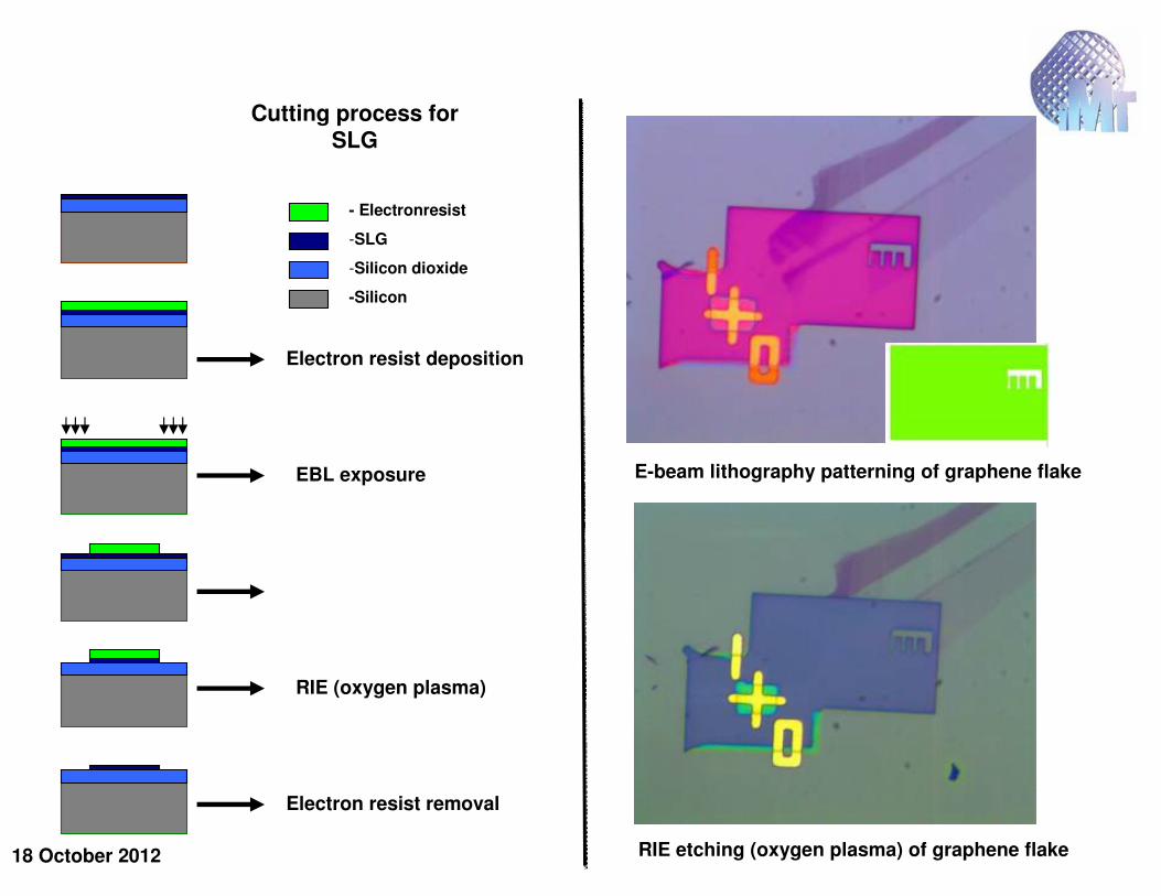
E-beam lithography patterning of graphene flake
RIE etching (oxygen plasma) of graphene flake
Electron resist deposition
EBL exposure
RIE (oxygen plasma)
Electron resist removal
Cutting process for SLG
- Electronresist
-SLG
-Silicon dioxide
-Silicon
18 October 2012
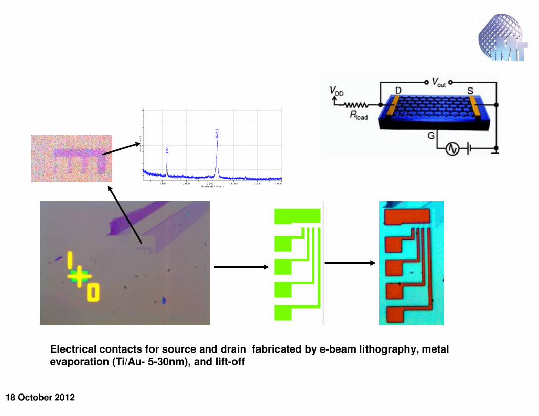
Electrical contacts for source and drain fabricated by e-beam lithography, metal evaporation (Ti/Au- 5-30nm), and lift-off
Inte
nsi
ty (
a. u.)
1 500 2 000 2 500 3 000 3 500 4 000Raman shift (cm-1)
1588.1
2642.8
18 October 2012
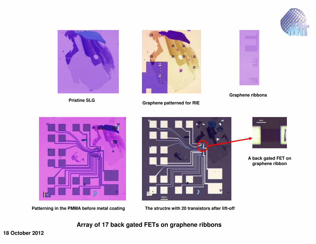
Graphene ribbonsPristine SLG
Graphene patterned for RIE
Patterning in the PMMA before metal coating The structre with 20 transistors after lift-off
A back gated FET on graphene ribbon
Array of 17 back gated FETs on graphene ribbons
18 October 2012
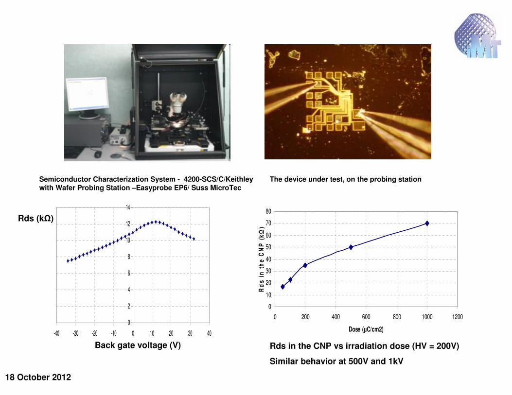
The device under test, on the probing stationSemiconductor Characterization System - 4200-SCS/C/Keithleywith Wafer Probing Station –Easyprobe EP6/ Suss MicroTec
0
2
4
6
8
10
12
14
-40 -30 -20 -10 0 10 20 30 40
Back gate voltage (V)
Rds (kΩ)
0
10
20
30
40
50
60
70
80
0 200 400 600 800 1000 1200
Dose (µC/cm2)
Rd
s i
n t
he
CN
P (
kΩ
)
Rds in the CNP vs irradiation dose (HV = 200V)
Similar behavior at 500V and 1kV
18 October 2012L. Gence, V. Callegari, A Dinescu, S. Melinte and S. Demoustier-Champagne, “Hybrid Polymer nanowire based electronic devices correlated characterization”
14-th International Conference of Modulated Semiconductor Structures (MSS 14), 19-24 July 2009, Kobe, Japan
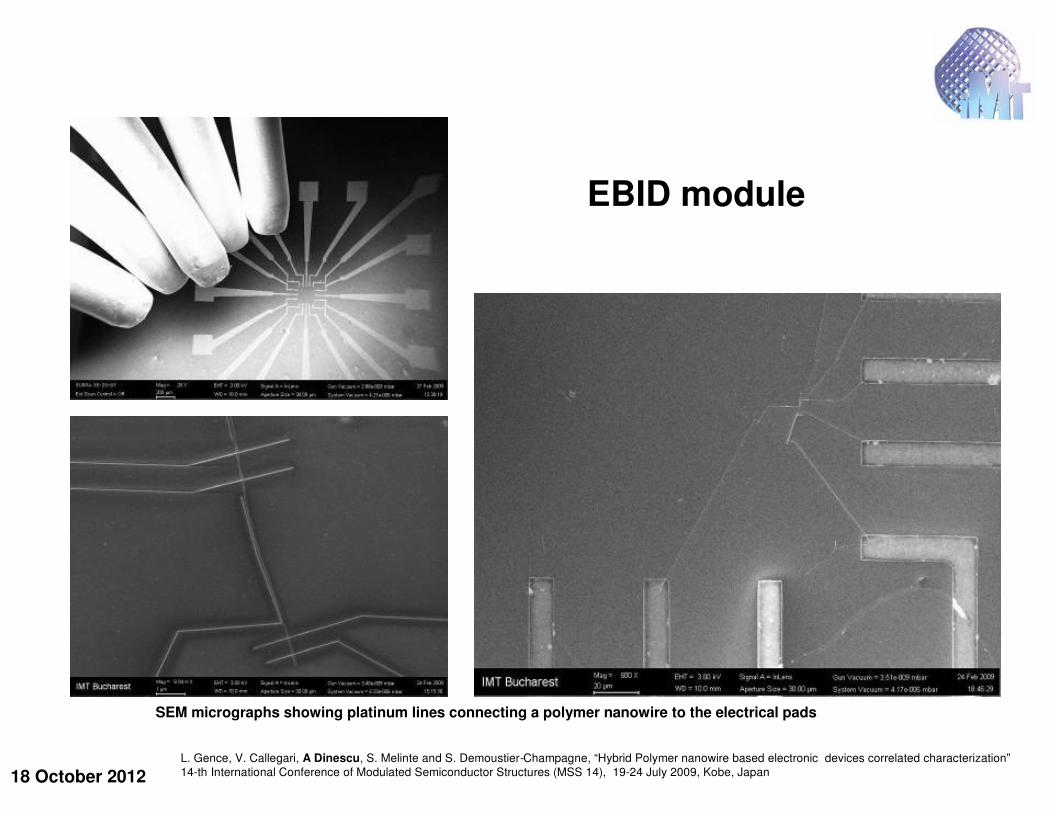
EBID module
SEM micrographs showing platinum lines connecting a polymer nanowire to the electrical pads
18 October 2012
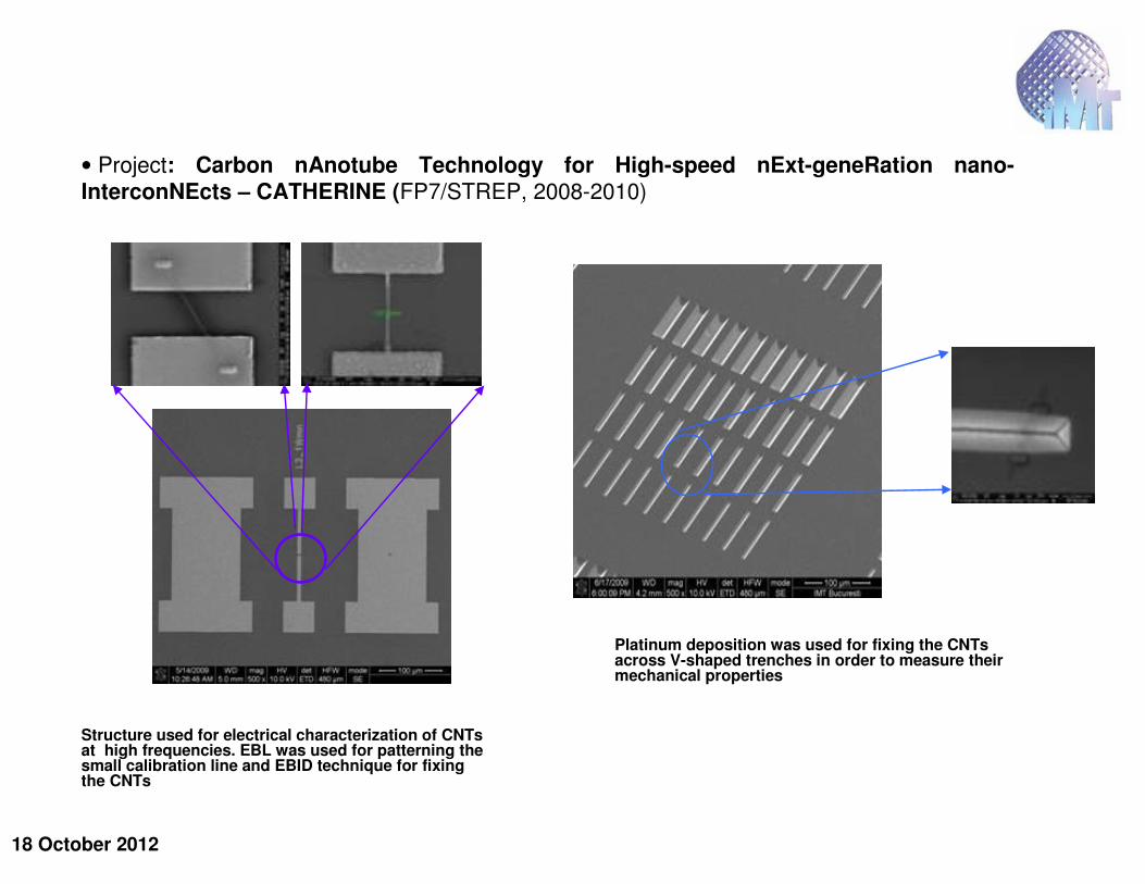
Structure used for electrical characterization of CNTs at high frequencies. EBL was used for patterning the small calibration line and EBID technique for fixing the CNTs
Platinum deposition was used for fixing the CNTs across V-shaped trenches in order to measure their mechanical properties
• Project: Carbon nAnotube Technology for High-speed nExt-geneRation nano-InterconNEcts – CATHERINE (FP7/STREP, 2008-2010)