Dispozitive si circuite electronice
45
DR PB. 1 2puncte D1 0.5 p a) Pentru v I1 =5V si v I2 =-5V, in ce stare sunt D1 si D2? Cum arata modelul circuitului in acest caz? 0.75p b) Care este expr esia v O (v I1 ,v I2 )? Cum arata cronograma v O (t) pentru v I1 (t) =1 0s in t [V] si v I2 =-10sin t [V]? Ce aplicatie realizeaza circuitul in acest caz? 0.5p c) Car e sunt valorile curentului direct maxim prin D 1, I F1max , si tensiunii inverse maxime pe D1, V rev1max pentru v I1 (t)=10sin t [V] si v I2 =-10sin t [V]? 0.25p d) Cum trebuie cuplat circuitul cu D1,D2, R L din figura (fara v I1 si v I2 ) la secundarul unui transformator cu priza mediana pentru a obtine un redresor bialternanta? A.1 Se considera D 1 si D 2 diode ideale: 0.5p. a) Care este fu nctia el ectrica v Y (v A ,v B ,v C ) ? 1p. b) v Y (t) pentru v C (t)=0; v A (t)=2V; v B (t)=5sin t [V]. Precizati starile de (c) si (b) ale D 1 si D 2 0.5p. c) v C =0V; v A ,v B {0v;10V}; 10V “1”logic; 0V “0”logic Care este tabelul de adevar Y(A,B) ? C.1 Se da circuitul din figura,D se considera dioda ideala: 0.5p. a) Cum arata CSTV v o (v I )? 0.5p. b) Cum arata v o (t) pentru v I =12sin t [V] ? 0.5p. c) In ce domeni u poate lua valor i R daca curentul maxim prin dio da este I dmax =50mA si v I este v I =12sin t [V]? 0.5p. d) Determinati CSTV daca in serie cu R s e introduce o sursa V pol =5V. Pb.1 Se da CSTV-ul pentru un diport DR, cu D ideala: 1p. a) Care este schema electrica a diportului DR ca sa se obtina CSTV-ul dat? 0.5p b) Cum arata v O (t) considerand v I (t) tens. triunghiulara cu amplitudinea de 3V si componenta continua 0V? 0.5p c) Pentru diportul de la punctul a) c um arata CSTV-ul considerand pentru di oda modelul cu V P =0.6V? 1. D1, D2 – ideal diodes 0.5p a) Find the expression of v Y (v A ,v B ,V Ref ). 0.5p b) For v A ,v B ∈{0V;10V} and V Ref =10V, fill in the voltage table and states of D1, D2 for all combinations of values of v A and v B . What is the logic function of the circuit assuming the logic convention: 0V-“0” logic; 10V-“1”logic? 0.5p c) Find the values of i D1 , i D2 and v D1 , v D2 for each of the 4 combinations of voltges v A , v B from (b). 0.5p d) For V Ref =0V, propose some waveforms for v A , v B to use this circuit as a full-wave voltage rectifier. What is the sign of the d.c. component of the output voltage v Y ? 2p P.1 Pentru circuitul din figura, rezistenta R=5k. 0.5p a) Determinati C STV v O (v I ) unde dioda D este considerata ideala; 0.5p b) Cronograma v O (t) pentru v I (t) – tensiune triunghiulara cu amplitudinea 7V si frecventa 100Hz; 1p c) Daca dioda D se considera reala cu caderea de tensiune in conductie v D = 0.7V cum arata CSTV si v O (t) pt. v I (t)=5sin1000t [V]? v I1 RL 10kΩ D2 v O v I2 A D2 v A R Y D1 B y v B v C R o D i v O v I 0 D R O v v I
-
Upload
ioana-paval -
Category
Documents
-
view
76 -
download
3
description
probleme la disciplina DCE.
Transcript of Dispozitive si circuite electronice

7/21/2019 Dispozitive si circuite electronice
http://slidepdf.com/reader/full/dispozitive-si-circuite-electronice-56d9365157aa2 1/45
DR
PB. 1 2puncteD1
0.5 p a) Pentru vI1=5V si vI2=-5V, in ce stare sunt D1 si D2? Cum arata modelul circuituluiin acest caz?0.75p b) Care este expresia vO(vI1,vI2)? Cum arata cronograma vO(t) pentru vI1(t)=10sin t[V] si vI2=-10sin t [V]? Ce aplicatie realizeaza circuitul in acest caz?0.5p c) Care sunt valorile curentului direct maxim prin D1, IF1max, si tensiunii inversemaxime pe D1, Vrev1max pentru vI1(t)=10sin t [V] si vI2=-10sin t [V]? 0.25p d) Cum trebuie cuplat circuitul cu D1,D2, R L din figura (fara vI1 si vI2) la secundarul unui transformator cu priza mediana pa obtine un redresor bialternanta?
A.1 Se considera D1 si D2 diode ideale:0.5p. a) Care este functia electrica vY(vA,vB,vC) ?1p. b) vY(t) pentru vC(t)=0; vA(t)=2V; vB(t)=5sin t [V].
Precizati starile de (c) si (b) ale D1 si D2 0.5p. c) vC=0V; vA,vB 0v;10V; 10V “1”logic; 0V “0”logic
Care este tabelul de adevar Y(A,B) ?
C.1 Se da circuitul din figura,D se considera dioda ideala:0.5p. a) Cum arata CSTV vo(vI)?0.5p. b) Cum arata vo(t) pentru vI=12sin t [V] ?0.5p. c) In ce domeniu poate lua valori R daca curentul maxim prin dioda
este Idmax=50mA si vI este vI=12sin t [V]?0.5p. d) Determinati CSTV daca in serie cu R se introduce
o sursa V pol=5V.
Pb.1 Se da CSTV-ul pentru un diport DR, cu D ideala:1p. a) Care este schema electrica a diportului DR ca sa se obtina CSTV-ul dat?
0.5p b) Cum arata vO(t) considerand v
I(t) tens. triunghiulara cu amplitudinea de 3V si componenta continua 0V?
0.5p c) Pentru diportul de la punctul a) cum arata CSTV-ul considerand pentru dioda modelul cu VP=0.6V?
1. D1, D2 – ideal diodes0.5p a) Find the expression of vY(vA,vB,VRef ).0.5p b) For vA,vB∈0V;10V and VRef =10V, fill in the voltage table and states of D1, D2 for allcombinations of values of vA and vB. What is the logic function of the circuit assuming the logicconvention: 0V-“0” logic; 10V-“1”logic?0.5p c) Find the values of iD1, iD2 and vD1, vD2 for each of the 4 combinations of voltges vA, vB from (b).0.5p d) For VRef =0V, propose some waveforms for vA, vB to use this circuit as a full-wave voltagerectifier. What is the sign of the d.c. component of the output voltage vY?
2p P.1Pentru circuitul din figura, rezistenta R=5k.
0.5p a) Determinati CSTV vO(vI) unde dioda D este considerata ideala;0.5p b) Cronograma vO(t) pentru vI(t) – tensiune triunghiulara cu
amplitudinea 7V si frecventa 100Hz;1p c) Daca dioda D se considera reala cu caderea de tensiune in conductie
vD= 0.7V cum arata CSTV si vO(t) pt. vI(t)=5sin1000t [V]?
vI1 R L 10k Ω
D2vO
vI2
A
D2v A
R
Y
D1
B
yvB
vC
R
oD i
vO
vI0
D
R
Ovv I

7/21/2019 Dispozitive si circuite electronice
http://slidepdf.com/reader/full/dispozitive-si-circuite-electronice-56d9365157aa2 2/45
0.5 p a) Cum arata schema echivalenta a circuitului daca D este blocata? Pentru ce subdomeniu de valori al vI apare starea de blocarD si care este valoarea lui vO in acest caz?0.5p b) Cum arata modelul circuitului daca D este in conductie? Pentru ce subdomeniu de valori al vI apare starea de conductie a Dcare este expresia vO(vI) in acest caz?0.5p c) Cum arata reprezentarea grafica a CSTV vO(vI) acircuitului pentru vI [-15V;15V] si D-ideala? Dar daca
4
3
210.5
-2
-6
0
vI[V]
vI apartine [-15V;15V] iar D-cadere de tensiune constanta? 0.5p d) Reprezentati grafic cronograma vO(t) pentru vI(t) dinfigura considerand D-ideala. Ce aplicatie realizeaza circuitul?Determinati valoarea tensiunii inverse maxime pe D si acurentului direct maxim prin D pentru acest vI(t)
D
vI
R=10k Ω
VPOL =2V
vO
1. 1.75p
Assume D – ideal.
-1
21
3
0-2
v
-3
45
-4-5
67
vI V1. c)
1.
vO
R=10 K Ω
D
VBias5V
vI
0.75p a) For vI∈[-12V;12V], what is the expression vO(vI)? Plot the VTC vO(vI), marking on the vI axis the interval correspondingto D – off and the interval corresponding to D – on. What is the equivalent circuit for: (1) D – on; (2) D – off?0.5p b) For the circuit in (a), plot vO(t) for vI(t) above. What is the application of the circuit? What is the change of vO(t) assuming Dconstant voltage drop model?0.5p c) Assume a load resistance R L=10 K is connected on the circuit’s output. How does vO(t) modify for vI(t) in (b), assuming Dideal? What are the disadvantages of using this structure (with the output on D)? Propose another D-R circuit structure tosame vO(t) as the one in (b) for D-ideal, improved from the point of view of the power consumption from vI.
2.5p 1 .
DVPOL =2V
vI R5k Ω
1p a) Deduceti si reprezentati grafic CSTV vO(vI) a circuitului pentru vI ∈ [-10V; 10V]in ipoteza:(1) D- ideala; (2) D- cadere de tensiune constanta.0.75p b) Cum arata vO(t), pentru fiecare din cele 2 modele ale D considerate la punctul a),daca vI(t)=4sinωt[V]? Ce aplicatie realizeaza circuitul? vO 0.75p c) La iesirea circuitului se conecteaza o rezistenta de sarcina R L=5K . Se modificaCSTV vO(vI) pentru noul circuit, considerand D- ideala fata de circuitul initial? Daca da,rededuceti CSTV vO(vI) pentru vI∈ [-10V; 10] si redesenati vO(t) pentru vI(t) de la punctul b).
7/21/2019 Dispozitive si circuite electronice
http://slidepdf.com/reader/full/dispozitive-si-circuite-electronice-56d9365157aa2 3/45
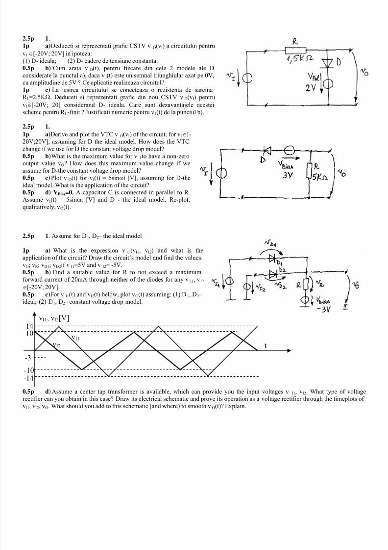
2.5p 1 .1p a) Deduceti si reprezentati grafic CSTV vO(vI) a circuitului pentruvI ∈[-20V; 20V] in ipoteza:(1) D- ideala; (2) D- cadere de tensiune constanta.0.5p b) Cum arata vO(t), pentru fiecare din cele 2 modele ale Dconsiderate la punctul a), daca vI(t) este un semnal triunghiular axat pe 0V,cu amplitudine de 5V ? Ce aplicatie realizeaza circuitul?1p c) La iesirea circuitului se conecteaza o rezistenta de sarcinaR L=2.5K . Deduceti si reprezentati grafic din nou CSTV vO(vI) pentruvI∈[-20V; 20] considerand D- ideala. Care sunt dezavantajele acesteischeme pentru R L-finit ? Justificati numeric pentru vI(t) de la punctul b).
2.5p 1.1p a) Derive and plot the VTC vO(vI) of the circuit, for vI∈ [-20V;20V], assuming for D the ideal model. How does the VTCchange if we use for D the constant voltage drop model?0.5p b) What is the maximum value for vI to have a non-zerooutput value vO? How does this maximum value change if weassume for D-the constant voltage drop model?0.5p c) Plot vO(t) for vI(t) = 5sinωt [V], assuming for D-theideal model. What is the application of the circuit?0.5p d) VBias =0. A capacitor C is connected in parallel to R.Assume vI(t) = 5sinωt [V] and D - the ideal model. Re-plot,qualitatively, vO(t).
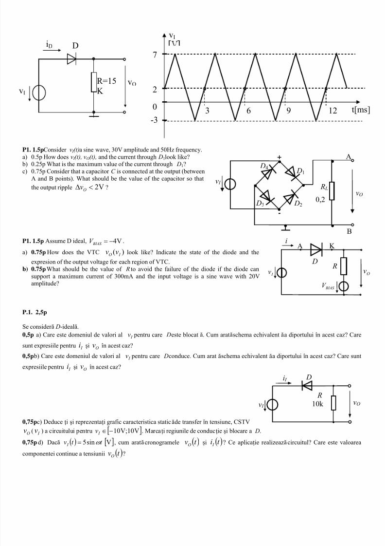
2.5p 1 . Assume for D1, D2 – the ideal model
1p a) What is the expression vO(vI1, vI2) and what is theapplication of the circuit? Draw the circuit’s model and find the values:vO; vR ; vD1; vD2 if vI1 =5V and vI2 = -5V.0.5p b) Find a suitable value for R to not exceed a maximumforward current of 20mA through neither of the diodes for any vI1, vI2 ∈[-20V; 20V].0.5p c) For vI1(t) and vI2(t) below, plot vO(t) assuming: (1) D1, D2 – ideal; (2) D1, D2 – constant voltage drop model.
vI1, vI2 [V]14
-14
10
-10
vI1 vI2 t
-3
0.5p d) Assume a center tap transformer is available, which can provide you the input voltages vI1, vI2. What type of voltarectifier can you obtain in this case? Draw its electrical schematic and prove its operation as a voltage rectifier through the tvI1, vI2, vO. What should you add to this schematic (and where) to smooth vO(t)? Explain.

7/21/2019 Dispozitive si circuite electronice
http://slidepdf.com/reader/full/dispozitive-si-circuite-electronice-56d9365157aa2 4/45
Pentru D1 , D2 se consider ă modelul diodă ideală.a) 0,75p Pentru circuitul din Figura 1.a, deduceţi şi reprezentaţi grafic CSTV vO(vI) a circuitului pentru ]V20;V20[vI −∈ . Caplicaţie realizează circuitul? Ilustraţi r ăspunsul prin cronogramele vI(t) şi vO(t) pentru vI(t)=15 sinωt [V].b) 0,75p Pentru circuitul din Figura 1.b, se aplică tensiunea vI=7V. În ce stări (conducţie sau blocare) sunt D1, respectiv D2? Cum aramodelul circuitului în acest caz? Ce valori au: vO; vD1; vD2; iD1; iD2? c) 0,5p Cum arată CSTV vO(vI) a circuitului din Figura 1.b pentru ]V20;V20[vI −∈ ? Pentru ce aplicaţie poate fi folosit circuidacă de exemplu vI(t)=15 sinωt [V]?
Assume D1, D2 - ideala) 0.75p What is the expression of vO(vA, vB)? Determine the value of vO, thecurrent iR , the states of D1 and D2 and the voltages on D1 and D2 for vA= - 1Vand vB = 8V. Draw the circuit’s model in this case.b) 0.5p Is it possible to use this circuit as a logic circuit with the inputs A andB, considering the following voltage levels: 0V – “0”; 10V – “1”? Whereshould be the output Y of the logic circuit? Find the suitable value of VBias touse the circuit as a logic circuit with these voltage levels and give the logictable of the circuit with inputs A, B and output Y. c) 0.5p Assume vA, vB are obtained from a center-tapped transformer: Find the expressions of vA(t), vB(t). Plot vA(t), vB(t) and vO(t). What is theapplication of the circuit?Compute: the maximum reverse voltage on D1 and the maximum forwardcurrent through D2.d) 0.25p What is the maximum variation of vO for the circuit in question(c)? Propose a solution to reduce this maximum variation. Will the maximumreverse voltage on D1 and the maximum forward current through D2 modifyin this case, and if yes, how?
D2
R=2K
vO
D1
v A
v B
~220V ef
n=44
R
D1• A
•
vO
BV
D2•
R2K
I RV A
V BIAS =3V •

7/21/2019 Dispozitive si circuite electronice
http://slidepdf.com/reader/full/dispozitive-si-circuite-electronice-56d9365157aa2 5/45
PB1 2p
0.75p a) Considerand D ideala, care este expresia vO(vI) pentru vI [-20V;20V]? Cum arata CSTV vO(vI) a circuitului? Desenati modelelecircuitului in urmatoarele situatii: (1)D-b; (2)D-c, specificand intervalelede valori vI pentru care este valid fiecare model.0.25p b) Pentru vI [-20V;20V] ce valori are: (1) curentul direct maxim prin D; (2) tensiunea inversa maxima pe D?0.75p c) Cum se modifica CSTV vO(vI) pentru vI [-20V;20V] fata desituatia de la punctul a) daca pentru D se considera modelul cadere detensiune constanta? Pentru fiecare din cele doua situatii: D-ideala si D -cadere de tensiune constanta, cum arata vO(t) pentru vI(t) semnal triunghiulacircuitul?
r simetric cu amplitudinea de 10 V? Ce aplicatie reali
0.25p d) Cum trebuie modificat circuitul din figura, prin conectarea inca unei ramuri D-V pol in circuit pentru a obtine un circuit carasigure dubla limitare a tensiunii vO la 5V pentru orice valoare vI in afara unui anumit interval de tensiune?
R Assume D ideal:0.5p. a) How does the VTC vo(vI) look like?0.5p. b) Plot vo(t) for vI=12sin t [V] ?0.5p. c) What is the range of possible values for R if the maximum forward diode
current is IDmax=50mA and vI is vI=12sin t [V]?0.5p. d) Determine the VTC if a dc biasing voltage source VBIAS=5V is introduced in circuit in series with R ?
P1. 2p . Se cunosc: domeniul de valori alv I ∈ [13;16]V, tipuldiodei Zener: PL10 Z, domeniul în care poate lua valori
R L∈ [350Ω; ∞] si R = 70Ω . a) 0.5p. Care este valoarea tensounii de iesire?b) 1p. Care sunt valorile minimeşi maxime ale curentuluii Z ?c) 0.5p . Care este puterea maxima disipata de dioda Zener?
P1. 2p . For the circuit we know the range ofv I ∈ [13;16]V, the type ofthe Zener diode: PL10 Z, the range of R L∈ [350Ω; ∞] and R = 70Ω . a) 0.5p. What is the value of the output voltage?b) 1p. What are the minimum and maximum values of thei Z current?c) 0.5p . What is the maximum power dissipated by the Zener diode?
P2. 2.5pa) Dacă vI∈[-7V; 7V], deduceţi expresia vO(vI) şi reprezentaţi grafic CSTV vO(vI) a circuitului în următoarele ipoteze: (1) D
ideală; (2) D – modelul cădere de tensiune constantă.b) Cum arată cronogramele vO(t) şi iD(t) în ipoteza D – ideală dacă vI(t) are cronograma din figur ă? Ce aplicaţie realizea
circuitul? d) Dacă la ieşirea circuitului, în paralel cu R, se conectează un condensator C de valoare 10μF, cum arată cronograma vO(t), î
ipoteza D – ideală, pentru vI(t) de la punctul (b)? Calculaţi variaţia maximă a tensiunii vO în regim permanentşi comparaaceastă variaţie cu variaţia maximă a tensiunii vO de la punctul (b).
v ov i D
v I
R
R L
i R I O
V O
i Z V Z ZD
v I
R
R L
i R I
i Z
ZD V Z
7/21/2019 Dispozitive si circuite electronice
http://slidepdf.com/reader/full/dispozitive-si-circuite-electronice-56d9365157aa2 6/45
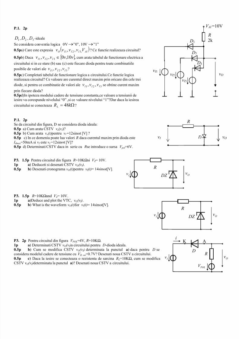
P1. 1.5p Considerv I (t) a sine wave, 30V amplitude and 50Hz frequency.a) 0.5p How doesv I (t), v O(t), and the current through D1 look like? b) 0.25p What is the maximum value of the current through D1?c) 0.75p Consider that a capacitorC is connected at the output (between
A and B points). What should be the value of the capacitor so thatthe output ripple V2< ?Δ
Ov
P1. 1.5p Assume D ideal, .V4−= BIAS V
a) 0.75p How does the VTC )( I O vv look like? Indicate the state of the diode and theexpresion of the output voltage for each region of VTC.
b) 0.75p What should be the value of R to avoid the failure of the diode if the diode cansupport a maximum current of 300mA and the input voltage is a sine wave with 20Vamplitude?
P.1. 2,5p
Se consider ă D-ideală.0,5p a) Care este domeniul de valori al pentru care D este blocată. Cum arată schema echivalentă a diportului în acest caz? Csunt expresiile pentru şi în acest caz?
I v
I i Ov0,5p b) Care este domeniul de valori al pentru care D conduce. Cum arată schema echivalentă a diportului în acest caz? Care expresiile pentru şi în acest caz?
I v
I i Ov
0,75p c) Deduceţi şi reprezentaţi grafic caracteristica statică de transfer în tensiune, CSTV( ) a circuitului pentru . Marcaţi regiunile de conducţie şi blocare a D. Ov I v [ V10;V10−∈
I v ]
v IvO
R10k
Di I
i
I v
D
K A
R
BIAS V
•
•
••
vO
v I R L
D4
D3 D2
D1
+
-
•
•
•
A
B
0,2
2
0
vI
3-3
12 t[m96
7
vO v
I
R=15
K
DiD
0,75p d) Dacă ( ) t t v I ω sin5= [ ]V , cum arată cronogramele ( )t vO şi ( )t i I ? Ce aplicaţie realizează circuitul? Care este valoa
componentei continue a tensiunii ?( )t vO
7/21/2019 Dispozitive si circuite electronice
http://slidepdf.com/reader/full/dispozitive-si-circuite-electronice-56d9365157aa2 7/45
v I 1 v I 2
D1
D2
R
vO
2k
v I 3
D3
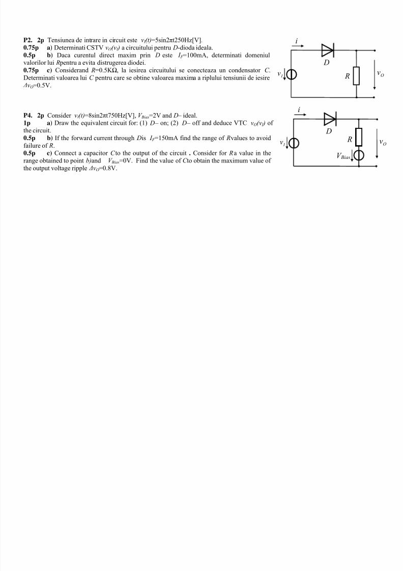
V Al =10VP.1. 2p
1 D , , -ideale2 D 3 DSe considera conventia logica 0V ”0”, 10V→ ”1”→
0.5p a) Care este expresia Al I I I O V vvvv ,321 ,, ? Ce functie realizeaza circuitul?
0.5p b) Daca , cum arata tabelul de functionare electrica acircuitului si in ce stare (b) sau (c) este fiecare dioda pentru toate combinatiile posibile de valori ale ?
vvvvv I I I 10,0,, 321 ∈
321 ,, I I I vvv
0.5p c) Completati tabelul de functionare logica a circuitului.Ce functie logicarealizeaza circuitul? Ce valoare are curentul direct maxim prin oricare din cele treidiode, si pentru ce combinatie de valori ale se obtine curent maxim prin fiecare dioda?
321 ,, I I I vvv
0.5p d)In ipoteza modului cadere de tensiune constanta,ce valoare a tensiunii deiesire va corespunde nivelului “0” ,si ce valoare nivelului “1”?Dar daca la iesireacircuitului se conecteaza ?Ω= k R L 48
P.1. 2p
vv I
R
D
Se da circuitul din figura, D se considera dioda ideala:0.5p a) Cum arata CSTVvo(v I )?0.5p b) Cum aratavo(t) pentruv I =12sinωt [V] ?0.5p c) In ce domeniu poate lua valori R daca curentul maxim prin dioda este
I dmax=50mA siv I estev I =12sinωt [V]?0.5p d) Determinati CSTV daca in serie cu R se introduce o sursaV pol =6V.
P3. 1.5p Pentru circuitul din figura R=10K Ω si V Z = 10V.
Ov I v R
DZ
1p a) Deduceti si desenati CSTVvO(v I ).0.5p b) Desenati cronograma vO(t) pentruv I (t)= 14sinωt[V].
P3. 1.5p R=10K Ω andV Z = 10V.1p a) Deduce and plot the VTC,vO(v I ).
Ov I v
R
DZ
0.5p b) What is the waveform vO(t) for v I (t)= 14sinωt[V].
iP3. 2p Pentru circuitul din figuraV POL =4V, R=10K Ω.1p a) Determinati CSTVvO(v I ) a circuitului pentru D-dioda ideala.0.5p b) Cum se modifica CSTVvO(v I ) determinata la punctula) daca pentru D seconsidera modelul cadere de tensiune cuV D, on =0.7V? Desenati noua CSTV a circuitului.0.5p c) Daca la iesire se conecteaza o rezistenta de sarcina R L=10K Ω, cum se modificaCSTVvO(v I ) determinata la punctula) ? Desenati noua CSTV a circuitului.
I v D
AK
R
POLV
7/21/2019 Dispozitive si circuite electronice
http://slidepdf.com/reader/full/dispozitive-si-circuite-electronice-56d9365157aa2 8/45
i
I v D
R
P2. 2p Tensiunea de intrare in circuit estev I (t)=5sin2πt250Hz[V].0.75p a) Determinati CSTVvO(v I ) a circuitului pentru D-dioda ideala.0.5p b) Daca curentul direct maxim prin D este I F =100mA, determinati domeniulvalorilor lui R pentru a evita distrugerea diodei.0.75p c) Considerand R=0.5K Ω, la iesirea circuitului se conecteaza un condensatorC .Determinati valoarea luiC pentru care se obtine valoarea maxima a riplului tensiunii de iesire Δ vO=0.5V.
i
I v D
R
V Bias
P4. 2p Considerv I (t)=8sin2πt750Hz[V],V Bias =2V and D – ideal.1p a) Draw the equivalent circuit for: (1) D – on; (2) D – off and deduce VTCvO(v I ) ofthe circuit.0.5p b) If the forward current through D is I F =150mA find the range of R values to avoidfailure of R.0.5p c) Connect a capacitorC to the output of the circuit. Consider for R a value in therange obtained to pointb) and V Bias =0V. Find the value ofC to obtain the maximum value ofthe output voltage ripple Δ vO=0.8V.
7/21/2019 Dispozitive si circuite electronice
http://slidepdf.com/reader/full/dispozitive-si-circuite-electronice-56d9365157aa2 9/45
DC
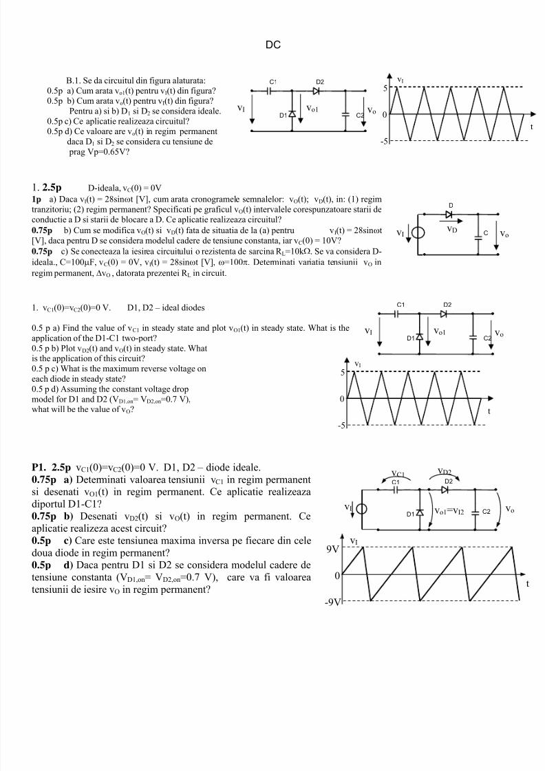
B.1. Se da circuitul din figura alaturata:5
-5
0
vI C1 D2
0.5p a) Cum arata v o1(t) pentru v I(t) din figura?
D
CvI vo vD
D2C1
C2D1 vI vo1=v I2 v
vC1 vD2
9V
-9V
0
vI
0.5p b) Cum arata v o(t) pentru v I(t) din figura?Pentru a) si b) D 1 si D 2 se considera ideale.
0.5p c) Ce aplicatie realizeaza circuitul?
0.5p d) Ce valoare are v o(t) in regim permanentdaca D 1 si D 2 se considera cu tensiune de prag Vp=0.65V?
1. 2.5p D-ideala, v C(0) = 0V1p a) Daca v I(t) = 28sin ω t [V], cum arata cronogramele semnalelor: v O(t); v D(t), in: (1) regimtranzitoriu; (2) regim permanent? Specificati pe graficul v O(t) intervalele corespunzatoare starii deconductie a D si starii de blocare a D. Ce aplicatie realizeaza circuitul?0.75p b) Cum se modifica v O(t) si v D(t) fata de situatia de la (a) pentru v I(t) = 28sin ω t[V], daca pentru D se considera modelul cadere de tensiune constanta, iar v C(0) = 10V?0.75p c) Se conecteaza la iesirea circuitului o rezistenta de sarcina R L=10k Ω . Se va considera D-ideala., C=100 μF, v C(0) = 0V, v I(t) = 28sin ω t [V], ω=100 π . Determinati variatia tensiunii v O inregim permanent, ΔvO , datorata prezentei R L in circuit.
1. v C1(0)=v C2(0)=0 V. D1, D2 – ideal diodes
0.5 p a) Find the value of v C1 in steady state and plot v O1(t) in steady state. What is theapplication of the D1-C1 two-port?0.5 p b) Plot v D2(t) and v O(t) in steady state. Whatis the application of this circuit?0.5 p c) What is the maximum reverse voltage oneach diode in steady state?0.5 p d) Assuming the constant voltage dropmodel for D1 and D2 (V D1,on = V D2,on =0.7 V),what will be the value of v O?
P1. 2.5p vC1(0)=v C2(0)=0 V. D1, D2 – diode ideale.0.75p a) Determinati valoarea tensiunii v C1 in regim permanentsi desenati v O1(t) in regim permanent. Ce aplicatie realizeazadiportul D1-C1?0.75p b) Desenati v D2(t) si v O(t) in regim permanent. Ceaplicatie realizeza acest circuit?
0.5p c) Care este tensiunea maxima inversa pe fiecare din celedoua diode in regim permanent?0.5p d) Daca pentru D1 si D2 se considera modelul cadere detensiune constanta (V D1,on = V D2,on =0.7 V), care va fi valoareatensiunii de iesire v O in regim permanent?
C2D1vI vo1 vo
D2C1
C2D1 vI vo1 vo
vI
0
-5
5
t
7/21/2019 Dispozitive si circuite electronice
http://slidepdf.com/reader/full/dispozitive-si-circuite-electronice-56d9365157aa2 10/45
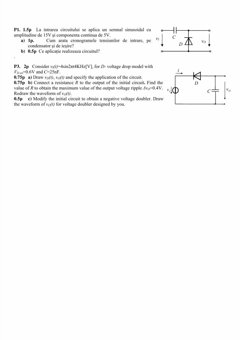
P1. 1.5p La intrarea circuitului se aplica un semnal sinusoidal cuamplitudine de 15V şi componenta continua de 5V.
v I vOC
D a) 1p. Cum arata cronogramele tensiunilor de intrare, pe
condensator şi de ie şire?b) 0.5p Ce aplica ţie realizeaza circuitul?
.
P3. 2p Consider v I (t)=4sin2 π t4KHz[V], for D- voltage drop model withV D,on =0.6V and C =25nF. i
I v D
C
0.75p a) Draw v D(t) , vO(t) and specify the application of the circuit.0.75p b) Connect a resistance R to the output of the initial circuit . Find thevalue of R to obtain the maximum value of the output voltage ripple Δ vO=0.4V.Redraw the waveform of vO(t) . 0.5p c) Modify the initial circuit to obtain a negative voltage doubler. Drawthe waveform of vO(t) for voltage doubler designed by you.
7/21/2019 Dispozitive si circuite electronice
http://slidepdf.com/reader/full/dispozitive-si-circuite-electronice-56d9365157aa2 11/45
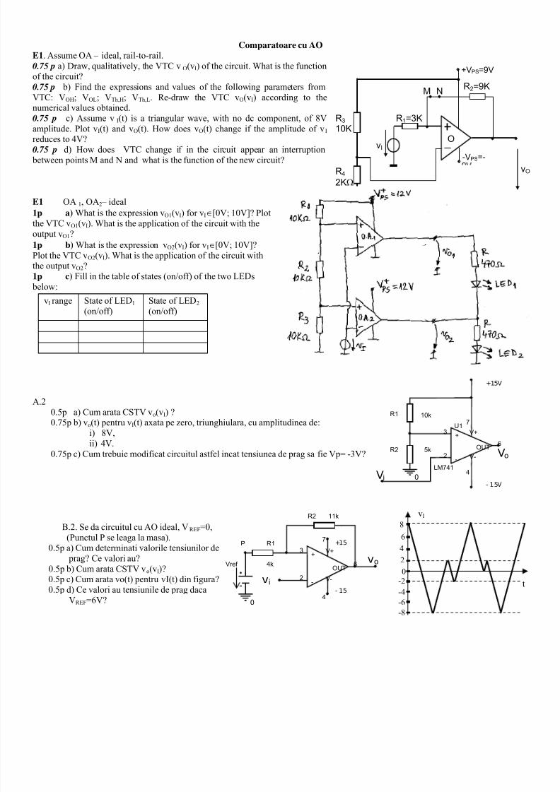
Comparatoare cu AOE1 . Assume OA – ideal, rail-to-rail.0.75 p a) Draw, qualitatively, the VTC v O(vI) of the circuit. What is the functionof the circuit?0.75 p b) Find the expressions and values of the following parameters fromVTC: V OH; V OL ; V Th,H ; V Th,L . Re-draw the VTC vO(v I) according to thenumerical values obtained.
0.75 p c) Assume v I(t) is a triangular wave, with no dc component, of 8Vamplitude. Plot v I(t) and v O(t). How does v O(t) change if the amplitude of v I reduces to 4V?0.75 p d) How does VTC change if in the circuit appear an interruption between points M and N and what is the function of the new circuit?
E1 OA 1, OA 2 – ideal1p a) What is the expression v O1(vI) for v I∈ [0V; 10V]? Plotthe VTC v O1(vI). What is the application of the circuit with theoutput v O1?1p b) What is the expression v O2(vI) for v I∈ [0V; 10V]?Plot the VTC v O2(vI). What is the application of the circuit withthe output v O2?
1p c) Fill in the table of states (on/off) of the two LEDs below:
A.2
0.5p a) Cum arata CSTV v o(v I) ?0.75p b) v o(t) pentru v I(t) axata pe zero, triunghiulara, cu amplitudinea de:i) 8V,ii) 4V.
0.75p c) Cum trebuie modificat circuitul astfel incat tensiunea de prag sa fie Vp= -3V?
B.2. Se da circuitul cu AO ideal, V REF =0,(Punctul P se leaga la masa).
0.5p a) Cum determinati valorile tensiunilor de prag? Ce valori au?
0.5p b) Cum arata CSTV v o(v I)?0.5p c) Cum arata vo(t) pentru vI(t) din figura?0.5p d) Ce valori au tensiunile de prag daca
VREF =6V?
vI range State of LED 1 (on/off)
State of LED 2 (on/off)
O
R 1 =3KR 3 10K
R 2 =9K
+V PS =9V
M N
v I
-V PS =-
vR 4
2K Ω
+15V
Vo
R1
10k
0
5k R2
Vi
7U1
- 15V
LM741
3 V++
2 4
6OUT
V--
-2
4
-6
2
6
8
0
-4t
vI
-8
R2 11k
- 15
R1
4k
v i
v o
3
2
7
4
6+
-
V+
V-
OUT
+15P
Vref
0

7/21/2019 Dispozitive si circuite electronice
http://slidepdf.com/reader/full/dispozitive-si-circuite-electronice-56d9365157aa2 12/45
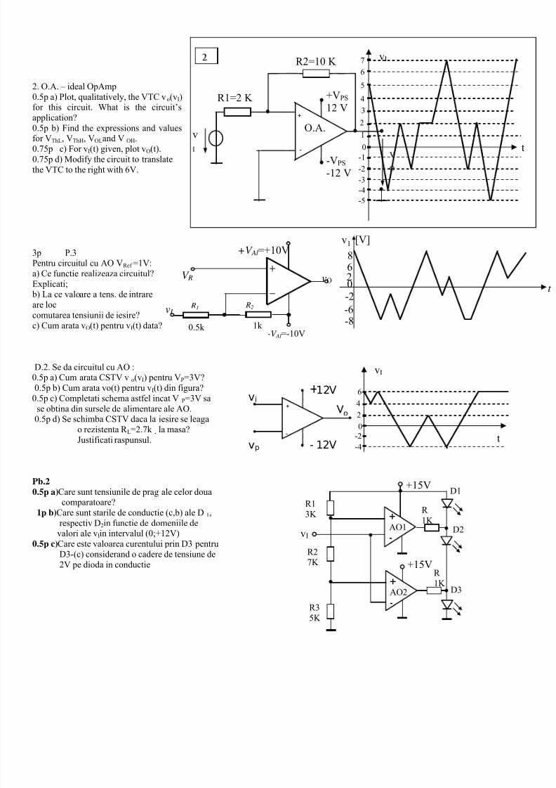
Assume O.A. – ideal
R1=3K
vI
+
-
R2=10K
O.A.
vO
+V P
S
12V
-V PS=-12VR310K
R42K
3.
VRe
f
0.75p a) Plot, qualitatively, the VTC v O(vI) of this circuit.Find the expressions and values of: V OL , VOH , VThL , VThH fromthe VTC v O(vI) of the circuit, and re-plot the VTC according tothe values obtained, for v I∈ [-10V;10V]. (Assume V Ref =-2V).0.5p b) For v I(t) = 7 sin ωt [V], plot v O(t). What is the applicationof the circuit? What would be v O(t) if the amplitude of v I(t) reduces to half?0.5p c) Modify the above circuit to allow the variation of the hysteresiswidth between [3V; 12V].
P2. 1.5p
Assume OA 1 , OA 2 ideal.a) 0.5p For v I∈ [-12V;12V], find the expression of v O1(v I) and plot the VTC v O1(vI). What is the application of the circuitassuming v O1 as output?b) 0.5p For v I∈ [-12V;12V], find the expression of v O2(v I) and plot the VTC v O2(vI). What is the application of the circuitassuming v O2 as output?c) 0.5p Plot the VTC v O(v I) for v I∈ [-12V;12V]. Assuming v I(t)=11 sin ω t [V], plot v I(t) and v O(t). What is the application of thecircuit?
2. 2p
+
vOvI
+V Al
12V
-VAl
-12V
R 3 10K Ω
R 4 20K Ω
-
R 1=5K Ω
R 2=20K Ω
AO
0.5p a) Cum arata calitativ graficul CSTV v O(vI) a circuitului? Ce aplicatierealizeaza circuitul?0.5p b) Gasiti expresiile si valorile urmatoarelor marimi de pe CSTV a circuitului:VOL , VOH , VPL, VPH.0.5p c) Cum arata v O(t) pentru v I(t) - semnal triunghiular simetric fata de 0, cuamplitudinea de 10V? Care este amplitudinea minima a semnalului triunghiular v I(t) pentru care obtinem la iesire un semnal semnal dreptunghiular? Justificati raspunsul.0.5p d) Daca in locul grupului (R 3, R 4) dispunem de un potentiometru P, cumtrebuie cuplat acest potentiometru in locul grupului (R 3, R 4) in circuit si pe ce pozitie trebuie sa fie cursorul P pentru a obtine aceeasi CSTV v O(v I) a circuitului? Ince consta modificarea CSTV v O(v I) regland cursorul potentiometrului P fata de cazulde la (a)?

7/21/2019 Dispozitive si circuite electronice
http://slidepdf.com/reader/full/dispozitive-si-circuite-electronice-56d9365157aa2 13/45
A.O. se consider ă ideal.a) 0,5p Cum arat ă, calitativ, CSTV v O(vI) a circuitului?Pentru ce tip de aplica ţii poate fi folosit circuitul?b) 0,5p Găsiţi expresiile şi valorile urm ătoarelor m ărimidin CSTV: V OH , V OL , V PH, V PL şi redesena ţi la scar ă CSTVvO(v I) în conformitate cu aceste valori numerice.c) 0,5p Reprezenta ţi cronogramele v O(t) şi v I(t) pentru v I(t) – triunghiular simetric, axat pe 0V, cu amplitudinea de 10V.d) 0,5p Ce valoare trebuie s ă aib ă tensiunea V Ref astfelîncât PLPH VV = ? Pentru aceast ă valoare a V Ref ,redimensiona ţi R 1 şi R 2 astfel încât l ăţimea histerezisului s ă se reduc ă la jum ătate fa ţă de circuitul din enun ţ. Ce valoriau în acest caz V PL şi VPH?
2.5p 2 . AO – ideal iar pt DZ, V Zo=5.1V. Se va considera V Z=const.=V Zo 0.5p a) Cum arata calitativ CSTV v O(vI) a circuitului ? Ce functierealizeaza circuitul ?1p b) Calculati urmatorii parametrii ai CSTV: V OH , V OL , V PH ,VPL. Redesenati CSTV la scara in conformitate cu valorile numericeobtinute.0.5p c) Cum arata v O(t) pentru v I(t) = 8sin ωt [V] ?0.5p d) Cum se modifica CSTV v O(vI) daca apare o intrerupere atraseului dintre intrarea (+) a AO si capatul din stanga al R 2 ? Justificatiraspunsul.
2.5p 2 .0.5p a) Draw, qualitatively, the VTC v O(v I) of the circuit. What is
the function of the circuit?1p b) Find the expressions and values of the following parameters from VTC: V OH; V OL; V Th,H ; V Th,L . Re-draw the VTC
vO(v I) according to the numerical values obtained.
1p c) Assume v I(t) is a triangular wave, with no D.C.component, of 10V amplitude (v I∈ [-10V;10V]). Plot v I(t) and v O(t).How does v O(t) change if the amplitude of v I reduces to 5V?
2.5p 2. Pentru AO 1, AO 2 – ideale1p a) Care este expresia v O1(vI) pentru v I∈ [0V; 10V]?Reprezentati grafic CSTVv O1(vI). Care este aplicatia realizata de
circuitul cu iesirea v O1?1p b) Care este expresia v O2(v I) pentru v I∈ [0V; 10V]?Reprezentati grafic CSTVv O2(vI). Care este aplicatia realizata decircuitul cu iesirea v O2?0.5p c) Completati tabelul de functionare cu starile celor douaLED-uri (conductie/blocare) pentru valorile corespunzatoare ale v I.
ValoareavI
LED 1 (c)/(b)
LED 2 (c)/(b)
AO1
+V AL =15V
-V AL =-15V
AO2
+V AL =15V
-V AL =-15V
R 1 =20K Ω
R 2 =20K Ω
R 3 =10K Ω
v I
v O1
v O2
LED1
R470 Ω
LED2
R470 Ω
7/21/2019 Dispozitive si circuite electronice
http://slidepdf.com/reader/full/dispozitive-si-circuite-electronice-56d9365157aa2 14/45
R1=2 K
vI
+
-
R2=10 K
O.A.
vO
+V PS
12 V
-VPS
-12 V
-1
2
1
3
0
-2
vI
-3
4
5
-4-5
67
2. O.A. – ideal OpAmp0.5p a) Plot, qualitatively, the VTC v o(v I)for this circuit. What is the circuit’sapplication?0.5p b) Find the expressions and valuesfor V ThL , VThH , VOL and V OH .0.75p c) For v I(t) given, plot v O(t).0.75p d) Modify the circuit to translatethe VTC to the right with 6V.
0268
-8-6-2
Iv [V]
-V Al=-10V
+V Al=+10V
0.5k
V R
1k
R2 R1
vO
v I
3p P.3Pentru circuitul cu AO V Ref =1V:
a) Ce functie realizeaza circuitul?Explicati; b) La ce valoare a tens. de intrareare loccomutarea tensiunii de iesire?c) Cum arata v O(t) pentru v I(t) data?
D.2. Se da circuitul cu AO :
-2
4
2
6
0
-4t
vI 0.5p a) Cum arata CSTV v o(v I) pentru V P=3V?0.5p b) Cum arata vo(t) pentru v I(t) din figura?
+
-
- 12V
o
v i
v p
12V 0.5p c) Completati schema astfel incat V P=3V sa
se obtina din sursele de alimentare ale AO.0.5p d) Se schimba CSTV daca la iesire se leaga
o rezistenta R L=2.7k la masa?Justificati raspunsul.
Pb.20.5p a) Care sunt tensiunile de prag ale celor doua
comparatoare?1p b) Care sunt starile de conductie (c,b) ale D 1,
respectiv D 2 in functie de domeniile devalori ale v I in intervalul (0;+12V)
0.5p c) Care este valoarea curentului prin D3 pentruD3-(c) considerand o cadere de tensiune de2V pe dioda in conductie
+15V
R13K
R27K
R35K
R1K
R1K
+AO2-
+AO1-
+15V
vI
D1
D2
D3

7/21/2019 Dispozitive si circuite electronice
http://slidepdf.com/reader/full/dispozitive-si-circuite-electronice-56d9365157aa2 15/45
D2
D1
-AO1
+12V-
AO2R3
R2
R1
+12V0.5p a) Care sunt tensiunile de prag ale celor doua
comparatoare?1p b) Care sunt starile de conductie (c,b) ale D 1,
respectiv D 2 in functie de domeniile de vI valori ale v I in intervalul (0;+12V)0.5p c) R=? astfel incat prin D1 si D2 sa treaca uncurent I=15mA considerand o cadere de 2V
pe diode in conductie directa.
Pentru circuitul cu AO de mai jos se dau: R1=1k, R2=5k,VRef = -10Va) Determinati tensiunile de prag ale circuitului V PH si V PL si CSTV v O(vI); b) Cum arata v O(t) pentru v I(t) data?c) Reproiectati circuitul a.i. cele doua praguri de comutare sa fie simetrice fata de zero.
2 R
0468
-8-6-2
v I [V]
-12
12
-4
-
101 R I v
Ov+
-
+10
-
V Ref R
R
R1=11 K
vI
+
-
R2=33 K
O.A.
+V PS
12 V
-VPS
-12 VR3=10 K
P=2.5 K
P2. 2.5p Assume O.A. – ideal.a) 0.5p Find the expression and range of values of the voltage on theinverting input of the O.A.Draw, qualitatively, the VTC v O(v I) of this circuit.b) 0.75p Find the expressions and values of the voltages V Th,L , VTh,H ,VOL and V OH from the VTC, assuming the position of the cursor of Pon its upper end.c) 0.5p How does the VTC modify if the cursor of P moves downtowards its lower end?d) 0.75p Plot v O(t) for v I(t) below, assuming the position of the cursorof P on its upper end. What is the application of the circuit?
20 t
vI [V]
45689
-2-4-5-6-8-9
7/21/2019 Dispozitive si circuite electronice
http://slidepdf.com/reader/full/dispozitive-si-circuite-electronice-56d9365157aa2 16/45
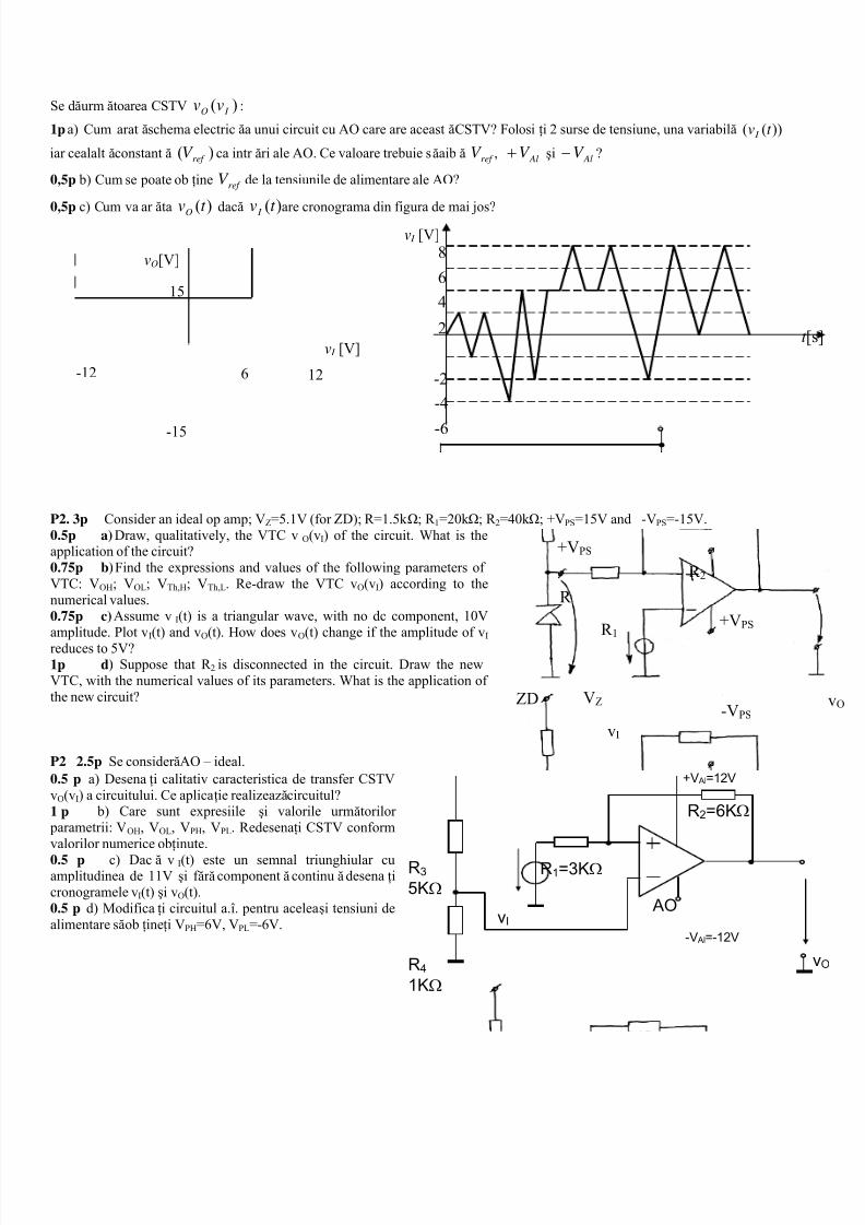
Se d ă urm ătoarea CSTV :)( I O vv1p a) Cum arat ă schema electric ă a unui circuit cu AO care are aceast ă CSTV? Folosi ţi 2 surse de tensiune, una variabil ă ))(( t v I
iar cealalt ă constant ă ca intr ări ale AO. Ce valoare trebuie s ă aib ă ,)( ref V ref V AlV + şi AlV − ?
0,5p b) Cum se poate ob ţine de la tensiunile de alimentare ale AO?ref V
0,5p c) Cum va ar ăta dac ă are cronograma din figura de mai jos?)(
t vO )(
t v I
v I [V]
t [
8
6
4
2
-2
-4
-6
v I [V]
vO [V]
15
-15
-12 6 12
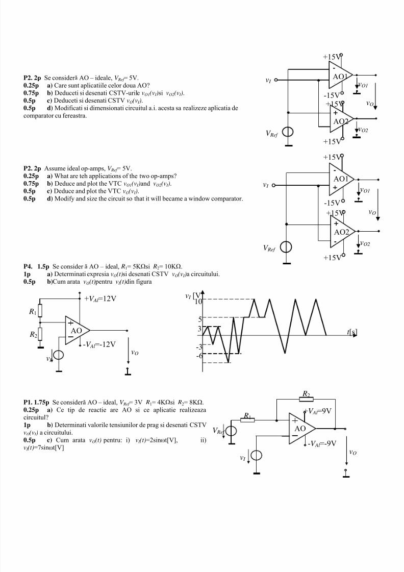
P2. 3p Consider an ideal op amp; V Z=5.1V (for ZD); R=1.5k Ω; R 1=20k Ω; R 2=40k Ω; +V PS=15V and -V PS=-15V.0.5p a) Draw, qualitatively, the VTC v O(vI) of the circuit. What is theapplication of the circuit?
ZD
R
R 1
R 2
+V PS
-VPS VZ
vI
ZD
R
R 1
R 2
+V PS
-V PS VZ
vI
+V PS 0.75p b) Find the expressions and values of the following parameters ofVTC: V OH ; V OL; V Th,H ; V Th,L . Re-draw the VTC vO(vI) according to thenumerical values.
0.75p c) Assume v I(t) is a triangular wave, with no dc component, 10Vamplitude. Plot v I(t) and v O(t). How does v O(t) change if the amplitude of v I reduces to 5V?1p d) Suppose that R 2 is disconnected in the circuit. Draw the newVTC, with the numerical values of its parameters. What is the application ofthe new circuit?
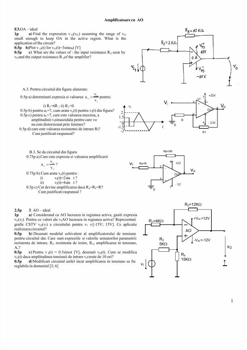
P2 2.5p Se consider ă AO – ideal. 0.5 p a) Desena ţi calitativ caracteristica de transfer CSTVvO(v I) a circuitului. Ce aplica ţie realizeaz ă circuitul?1 p b) Care sunt expresiile şi valorile urm ătorilor parametrii: V OH , V OL , V PH, V PL. Redesena ţi CSTV conformvalorilor numerice ob ţinute.0.5 p c) Dac ă v I(t) este un semnal triunghiular cuamplitudinea de 11V şi f ăr ă component ă continu ă desena ţicronogramele v I(t) şi vO(t).0.5 p d) Modifica ţi circuitul a.î. pentru acelea şi tensiuni dealimentare s ă ob ţine ţi VPH=6V, V PL=-6V.
AO
R 1 =3K ΩR 3
5K Ω
R 2 =6K Ω
+V Al =12V
-V Al =-12V
R 4
1K
v I
Ω
7/21/2019 Dispozitive si circuite electronice
http://slidepdf.com/reader/full/dispozitive-si-circuite-electronice-56d9365157aa2 17/45
+15V
+AO2
-AO1
+15V
v I vO1
vO2
-15V
+15V
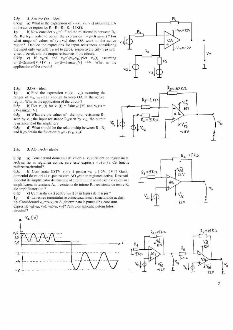
vO
V Ref
P2. 2p Se consider ă AO – ideale, V Ref = 5V.0.25p a) Care sunt aplicatiile celor doua AO? 0.75p b) Deduceti si desenati CSTV-urile vO1(v I ) si vO2(v I ). 0.5p c) Deduceti si desenati CSTV vO(v I ).0.5p d) Modificati si dimensionati circuitul a.i. acesta sa realizeze aplicatia decomparator cu fereastra.
+15V
+AO2-
-AO1
+15V
v I vO1
vO2
-15V
+15V
vO
V Ref
P2. 2p Assume ideal op-amps, V Ref = 5V.0.25p a) What are teh applications of the two op-amps? 0.75p b) Deduce and plot the VTC vO1(v I ) and vO2(v I ). 0.5p c) Deduce and plot the VTC vO(v I ).
0.5p d) Modify and size the circuit so that it will became a window comparator.
P4. 1.5p Se consider ă AO – ideal, R1= 5K Ω si R2= 10K Ω.1p a) Determinati expresia vO(t) si desenati CSTV vO(v I ) a circuitului. 0.5p b) Cum arata vO(t) pentru v I (t) din figura
v I [V]
t [s]
10
5
3
-3
-6
AO
R1
R2
+V Al=12V
-V Al=-12V
v I vO
R2 P1. 1.75p Se consider ă AO – ideal, V Ref = 3V R1= 4K Ω si R2= 8K Ω.0.25p a) Ce tip de reactie are AO si ce aplicatie realizeazacircuitul?1p b) Determinati valorile tensiunilor de prag si desenati CSTVvO(v I ) a circuitului.0.5p c) Cum arata vO(t) pentru: i) v I (t)=2sin ωt[V], ii)v I (t)=7sin ωt[V]
AO
R1 +V Al=9V
-V Al=-9V
V Ref
v I vO

7/21/2019 Dispozitive si circuite electronice
http://slidepdf.com/reader/full/dispozitive-si-circuite-electronice-56d9365157aa2 18/45
OA
R1
R2
+V Ps =12V
-V PS =-12V
V Ref vO
v I
P2. 2p Assume OA – ideal, V Ref = 4.5V R1= 3K Ω si R2= 9K Ω.0.25p a) What is the sign of circuit feedback and what is theapplication of the circuit?0.75p b) Compute the threshold voltages and draw VTC vO(v I ) of thecircuit.0.5p c) Draw the waveforms of vO(t) for: i) v I (t)=1.1sin ωt[V], ii)v I (t)=11sin ωt[V].0.5p d) Redesign the circuit to obtain V ThL= -6V and V ThH = 2V.
+15V
R310K
R28K
R12K
R
R
-OA2+
-OA1
+
+15V
v I D
D2
vO1
vO2
P3. 1.5p Assume both OA – ideal.0.25p a) What are the applications of each OAs?0.75p b) Compute the threshold voltages of the circuit and draw both VTC vO1(v I ) and vO2(v I ).0.5p c) What are the state of both diodes D1, D2 (on, off) depending on t
values of v I in the range (0;+15V)?
he
7/21/2019 Dispozitive si circuite electronice
http://slidepdf.com/reader/full/dispozitive-si-circuite-electronice-56d9365157aa2 19/45
Amplificatoare cu AO
E3. OA – ideal1p a) Find the expression v O(vI1) assuming the range of v I1 small enough to keep OA in the active region. What is theapplication of the circuit?0.5p b) Plot v O(t) for v I1(t)=3sin ω0t [V]0.5p c) What are the values of : the input resistance R i1 seen byvI1 and the output resistance R o of the amplifier?
A.3. Pentru circuitul din figura alaturata:
0.5p a) determinati expresia si valoareai
ov v
va = pentru:
i) R 1=6R ; ii) R 1=0.0.5p b) pentru a v=7, cum arata v o(t) pentru v i(t) din figura?0.5p c) pentru a v=7, care este valoarea maxima, a
amplitudinii v I sinusoidala pentru care vonu este distorsionat prin limitare?
0.5p d) care este valoarea rezistentei de intrare Ri?Cum justificati raspunsul?
B.3. Se da circuitul din figura:0.75p a) Care este expresia si valoarea amplificarii
i
ov v
va = ?
0.75p b) Cum arata v o(t) pentru :i) vI(t)=2sin t ?
ii) vI(t)=4sin t ?0.5p c) Cat devine amplificarea daca R a=R b=R?Cum justificati raspunsul ?
2.5p 3 . AO – ideal1p a) Considerand ca AO lucreaza in regiunea activa, gasiti expresiavO(v I). Pentru ce valori ale v I AO lucreaza in regiunea activa? Reprezentatigrafic CSTV v O(v I) a circuitului pentru v I ∈ [-15V; 15V]. Ce aplicatierealizeaza circuitul?0.5p b) Desenati modelul echivalent al amplificatorului de tensiune pentru circuitul dat. Care sunt expresiile si valorile urmatorilor parametrii:rezistenta de intrare, R i; rezistenta de iesire, R o; amplificarea in tensiune,Av?0.5p c) Pentru v I(t) = 0.5sin ωt [V], desenati v O(t). Cum se modificavO(t) daca amplitudinea tensiunii de intrare v i creste de 10 ori?0.5p d) Modificati circuitul astfel incat amplificarea in tensiune sa fiereglabila in domeniul [3; 6]
-1.5 t
vi
21.5
0
-2
Vo
0
U13
2
7
4
6
+
-
V+
V-
OUT
R1
+21V
i
R - 21V
Rb=5R
- 12
Ra=Rv i
v o
3
2
7
4
6
+
-
OUT
+12
0
AO
R 1=4K Ω
R 3
5KΩ
R 2=12K Ω
+V AL=12V
-V AL=-12V
vI
vO
R 4 15K Ω
7/21/2019 Dispozitive si circuite electronice
http://slidepdf.com/reader/full/dispozitive-si-circuite-electronice-56d9365157aa2 20/45
2.5p 2 . Assume OA – ideal0.75p a) What is the expression of v O(vI1,vI2, v I3) assuming OAin the active region for R 1=R 2=R 3=R 4=15K Ω?1p b) Now consider v I3=0. Find the relationship between R 1,R 2, R 3, R 4 in order to obtain the expression : v O=3(v I2-vI1) ? Forwhat range of values of (v I2-v I1) does OA work in the activeregion? Deduce the expresions for input resistances consideringthe input only v I1 (with v I2 set to zero), respectively only v I2 (withvI1 set to zero), and the output resistance of the circuit.0.75p c) If v I3=0 and v O=3(v I2-v I1) plot v O(t) assumingvI1(t)=2sin ω0t[V]+1V si v I2(t)=-3sin ω0t[V] +4V. What is theapplication of the circuit?
2.5p 3. OA – ideal1p a) Find the expression v O(vI1, v I2) assuming theranges of v I1, v I2 small enough to keep OA in the activeregion. What is the application of the circuit?0.5p b) Plot v O(t) for v I1(t) = 3sin ω0t [V] and v I2(t) =3V-2sin ω0t [V].
0.5p c) What are the values of : the input resistance R i1 seen by v I1; the input resistance R i2 seen by v I2; the outputresistance R o of the amplifier?0.5p d) What should be the relationship between R 1, R 2 and R 3 to obtain the function: v O = - (v I1+vI2)?
2.5p 3 . AO 1, AO 2 – ideale
0. 5p a) Considerand domeniul de valori al v I1 suficient de ingust incatAO 1 sa fie in regiunea activa, care este expresia v O(v I1) ? Ce functierealizeaza circuitul?0.5p b) Cum arata CSTV v
O(v
I1) pentru v
I1 ∈ [-5V; 5V] ? Gasiti
domeniul de valori al v I1 pentru care AO 1 este in regiunea activa. Desenatimodelul de amplificator de tensiune al circuitului in acest caz. Ce valori au :amplificarea in tensiune A v, rezistenta de intrare R i ; rezistenta de iesire R o ale amplificatorului ?0.5p c) Cum arata v O(t) pentru v I1(t) ca in figura de mai jos ?1p d) La iesirea circuitului se conecteaza inca o structura de acelasitip. Considerand v O1=A vvI1 cu A v determinata la punctul b), care suntexpresiile v O(vO1, v I2); v O(vI1, v I2)? Pentru ce aplicatie putem folosicircuitul?
OA
R 1
R 3
R 2
+VPS =12V
-VPS =-12V
vI2
vO
R 4
vI1
vI3
7/21/2019 Dispozitive si circuite electronice
http://slidepdf.com/reader/full/dispozitive-si-circuite-electronice-56d9365157aa2 21/45
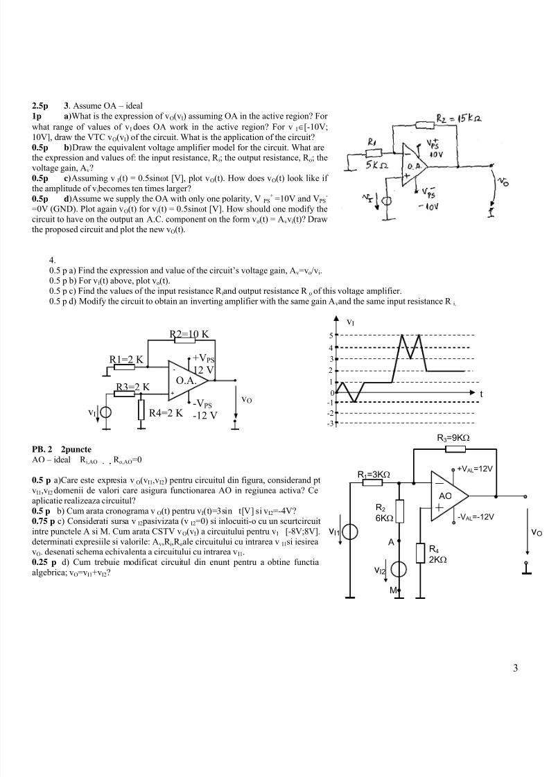
2.5p 3 . Assume OA – ideal1p a) What is the expression of v O(v I) assuming OA in the active region? Forwhat range of values of v I does OA work in the active region? For v I∈ [-10V;10V], draw the VTC v O(vI) of the circuit. What is the application of the circuit?0.5p b) Draw the equivalent voltage amplifier model for the circuit. What arethe expression and values of: the input resistance, R i; the output resistance, R o; thevoltage gain, A v?0.5p c) Assuming v I(t) = 0.5sin ωt [V], plot v O(t). How does v O(t) look like ifthe amplitude of v i becomes ten times larger?0.5p d) Assume we supply the OA with only one polarity, V PS
+ =10V and V PS-
=0V (GND). Plot again v O(t) for v i(t) = 0.5sin ωt [V]. How should one modify thecircuit to have on the output an A.C. component on the form v o(t) = A vvi(t)? Drawthe proposed circuit and plot the new v O(t).
4.
0.5 p a) Find the expression and value of the circuit’s voltage gain, A v=vo/v i.0.5 p b) For v i(t) above, plot v o(t).0.5 p c) Find the values of the input resistance R i and output resistance R o of this voltage amplifier.0.5 p d) Modify the circuit to obtain an inverting amplifier with the same gain A v and the same input resistance R i.
-1
21
3
0
-2
t
vI
-3
4
5
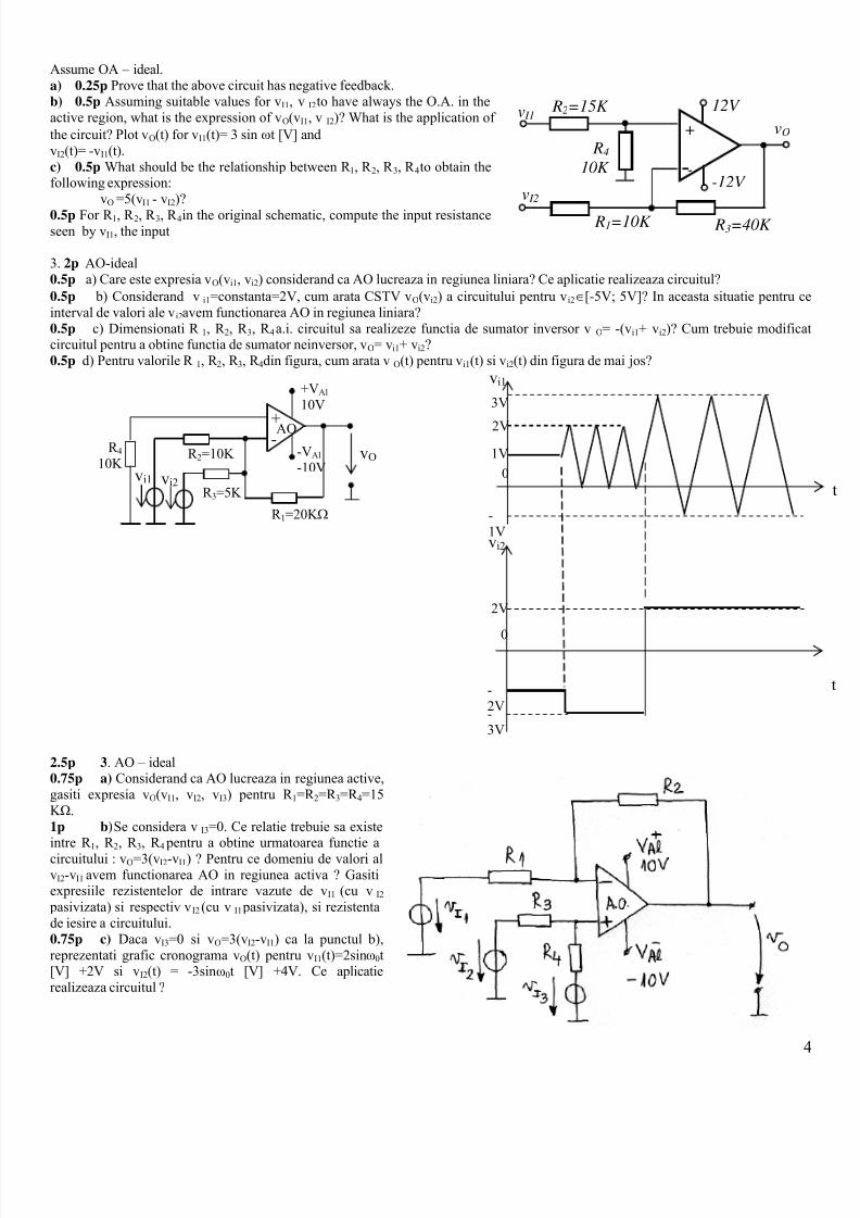
PB. 2 2puncteAO – ideal R i,AO R o,AO =0
0.5 p a)Care este expresia v O(v I1,v I2) pentru circuitul din figura, considerand ptvI1,vI2 domenii de valori care asigura functionarea AO in regiunea activa? Ceaplicatie realizeaza circuitul? 0.5 p b) Cum arata cronograma v O(t) pentru v I(t)=3sin t[V] si v I2=-4V?0.75 p c) Considerati sursa v I2 pasivizata (v I2=0) si inlocuiti-o cu un scurtcircuitintre punctele A si M. Cum arata CSTV v O(vI) a circuitului pentru v I [-8V;8V].
determinati expresiile si valorile: A v,R i,R o ale circuitului cu intrarea v I1 si iesireavO. desenati schema echivalenta a circuitului cu intrarea v I1.0.25 p d) Cum trebuie modificat circuitul din enunt pentru a obtine functiaalgebrica; v O=v I1+v I2?
R1=2 K
vI
+
-
R2=10 K
O.A.R3=2 K
R4=2 K
+V PS
12 V
-VPS-12 V
vO
AO
R 1=3K Ω
R 2 6KΩ
R 3=9K Ω
+V AL=12V
-V AL=-12V
A
M
vI2
vI1
R 4 2KΩ
7/21/2019 Dispozitive si circuite electronice
http://slidepdf.com/reader/full/dispozitive-si-circuite-electronice-56d9365157aa2 22/45
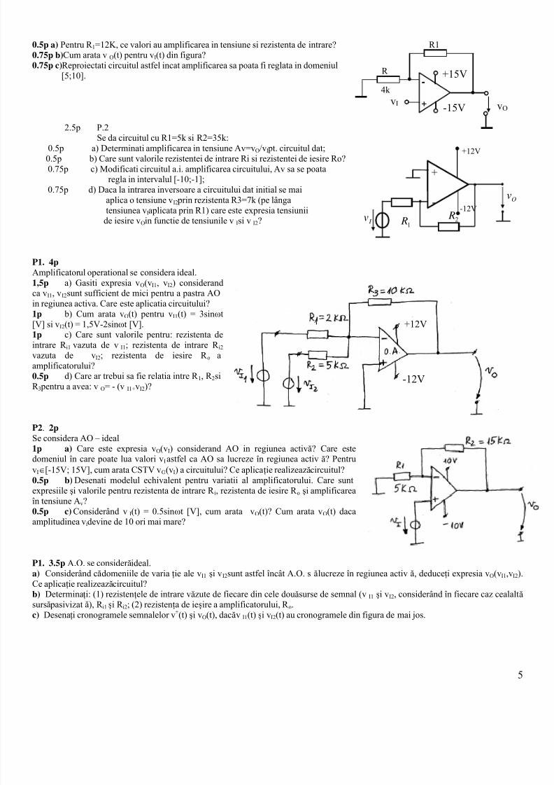
Assume OA – ideal.a) 0.25p Prove that the above circuit has negative feedback.b) 0.5p Assuming suitable values for v I1 , v I2 to have always the O.A. in theactive region, what is the expression of v O(v I1 , v I2)? What is the application ofthe circuit? Plot v O(t) for v I1(t)= 3 sin ω t [V] and vO
v I1
v I2
R4
10K
R3=40K
R2=15K
R1=10K
-
+
12V
-12V
vI2(t)= -v I1(t).c) 0.5p What should be the relationship between R 1, R 2, R 3, R 4 to obtain thefollowing expression:
vO =5(v I1 - v I2)?0.5p For R 1, R 2, R 3, R 4 in the original schematic, compute the input resistanceseen by v I1, the input
3. 2p AO-ideal0.5p a) Care este expresia v O(v i1, v i2) considerand ca AO lucreaza in regiunea liniara? Ce aplicatie realizeaza circuitul?0.5p b) Considerand v i1=constanta=2V, cum arata CSTV v O(v i2) a circuitului pentru v i2∈ [-5V; 5V]? In aceasta situatie pentru ceinterval de valori ale v i2 avem functionarea AO in regiunea liniara?0.5p c) Dimensionati R 1, R 2, R 3, R 4 a.i. circuitul sa realizeze functia de sumator inversor v O= -(v i1+ v i2)? Cum trebuie modificatcircuitul pentru a obtine functia de sumator neinversor, v O= v i1+ v i2?
0.5p d) Pentru valorile R 1, R 2, R 3, R 4 din figura, cum arata v O(t) pentru v i1(t) si v i2(t) din figura de mai jos?
vi1
3V
2V
1V
-1V
0
vi2
2V
-2V
0
-3V
+
vO
vi2
+V Al
10V
-VAl
-10V
R 2=10K
R 1=20K Ω
- R 4 10K
R 3=5Kvi1
AO
2.5p 3 . AO – ideal0.75p a) Considerand ca AO lucreaza in regiunea active,gasiti expresia v O(v I1, v I2, v I3) pentru R 1=R 2=R 3=R 4=15K Ω.1p b) Se considera v I3=0. Ce relatie trebuie sa existeintre R 1, R 2, R 3, R 4 pentru a obtine urmatoarea functie acircuitului : v O=3(v I2-vI1) ? Pentru ce domeniu de valori alvI2-vI1 avem functionarea AO in regiunea activa ? Gasitiexpresiile rezistentelor de intrare vazute de v I1 (cu v I2 pasivizata) si respectiv v I2 (cu v I1 pasivizata), si rezistentade iesire a circuitului.0.75p c) Daca v I3=0 si v O=3(v I2-vI1) ca la punctul b),reprezentati grafic cronograma v O(t) pentru v I1(t)=2sin ω0t[V] +2V si v I2(t) = -3sin ω0t [V] +4V. Ce aplicatierealizeaza circuitul ?
7/21/2019 Dispozitive si circuite electronice
http://slidepdf.com/reader/full/dispozitive-si-circuite-electronice-56d9365157aa2 23/45
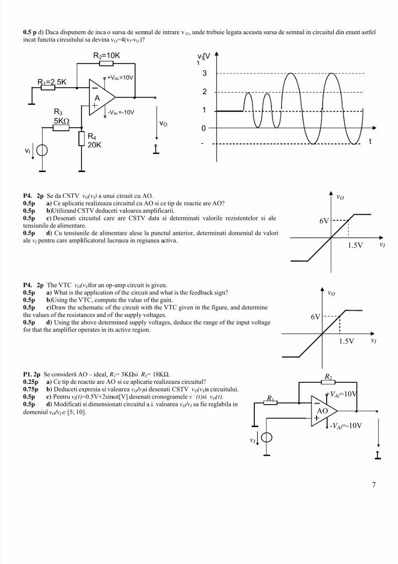
0.5p a) Pentru R 1=12K, ce valori au amplificarea in tensiune si rezistenta de intrare?
-
+
+15V
vI -15V
R1
R
vO
4k
0.75p b) Cum arata v O(t) pentru v I(t) din figura?0.75p c) Reproiectati circuitul astfel incat amplificarea sa poata fi reglata in domeniul
[5;10].
2.5p P.2Se da circuitul cu R1=5k si R2=35k:
0.5p a) Determinati amplificarea in tensiune Av=v O/vI pt. circuitul dat;
2 R
Ov
+
-
I v1 R
+12V
-12V
0.5p b) Care sunt valorile rezistentei de intrare Ri si rezistentei de iesire Ro?0.75p c) Modificati circuitul a.i. amplificarea circuitului, Av sa se poata
regla in intervalul [-10;-1];0.75p d) Daca la intrarea inversoare a circuitului dat initial se mai
aplica o tensiune v I2 prin rezistenta R3=7k (pe lângatensiunea v I aplicata prin R1) care este expresia tensiunii
de iesire v O in functie de tensiunile v I si v I2?
P1. 4p
Amplificatorul operational se considera ideal.1,5p a) Gasiti expresia v O(vI1, v I2) considerandca v I1, v I2 sunt sufficient de mici pentru a pastra AOin regiunea activa. Care este aplicatia circuitului?1p b) Cum arata v O(t) pentru v I1(t) = 3sin ωt[V] si v I2(t) = 1,5V-2sin ωt [V].1p c) Care sunt valorile pentru: rezistenta deintrare R i1 vazuta de v I1; rezistenta de intrare R i2 vazuta de v I2; rezistenta de iesire R o aamplificatorului?
+12V
-12V0.5p d) Care ar trebui sa fie relatia intre R 1, R 2 siR 3 pentru a avea: v O = - (v I1+vI2)?
P2 . 2pSe considera AO – ideal1p a) Care este expresia v O(v I) considerand AO in regiunea activ ă? Care estedomeniul în care poate lua valori v I astfel ca AO sa lucreze în regiunea activ ă? PentruvI∈ [-15V; 15V], cum arata CSTV v O(vI) a circuitului? Ce aplica ţie realizeaz ă circuitul?0.5p b) Desenati modelul echivalent pentru variatii al amplificatorului. Care suntexpresiile şi valorile pentru rezistenta de intrare R i, rezistenta de iesire R o şi amplificareaîn tensiune A v?0.5p c) Considerând v I(t) = 0.5sin ωt [V], cum arata v O(t)? Cum arata v O(t) dacaamplitudinea v i devine de 10 ori mai mare?
P1. 3.5p A.O. se consider ă ideal.a) Considerând c ă domeniile de varia ţie ale v I1 şi v I2 sunt astfel încât A.O. s ă lucreze în regiunea activ ă, deduce ţi expresia v O(vI1,vI2
Ce aplica ţie realizeaz ă circuitul?b) Determina ţi: (1) rezisten ţele de intrare v ăzute de fiecare din cele dou ă surse de semnal (v I1 şi v I2, considerând în fiecare caz cealaltsurs ă pasivizat ă), R i1 şi R i2; (2) rezisten ţa de ie şire a amplificatorului, R o.c) Desena ţi cronogramele semnalelor v +(t) şi vO(t), dac ă vI1(t) şi v I2(t) au cronogramele din figura de mai jos.

7/21/2019 Dispozitive si circuite electronice
http://slidepdf.com/reader/full/dispozitive-si-circuite-electronice-56d9365157aa2 24/45
d) Ce rela ţie ar trebui s ă existe între valorilerezisten ţelor R 1, R 2, R 3 şi R 4 astfel încât circuitul s ă realizeze dublul sumei algebrice a semnalelor v I1 şi v I2
R1=1.5 K
vI1
-
+
R2=27 K
A. O.vO
+V Al
10 V
-VAl
-10 V
vI2
R3
15 K R410 K v+
-0.5
-10
t
vI1 [V]1
0t
vI2 [V]1
R 1
R 3
R 2
+VPS =12
-VPS =-
vI2
vO
R 4
vI1
vI3
P2. 3p Assume an ideal op amp.1p a) What is the expression of v O(vI1,vI2,vI3) assuming OA in the activeregion for R 1=R 4=15K Ω ; R 2= R 3=30K Ω? What is the application of thecircuit?0.5p b) Redesign the circuit to obtain the expression v O = (-3v I1+2v I2 +2v I3)?0.5p c) If v I2=0, draw the VTC v O(v I3-vI1) of the circuit. For what range ofvalues of (v I3-vI1) does OA work in the active region?0.5p d) If v I2=0, plot v O(t) assuming v I1(t)=3sin ω0t[V] and v I3(t)=-4V.0.5p e) If v I2=0, deduce the expresions for input resistances seen by v I1,respectively by v I3, and the output resistance of the circuit.
.
P2. 2.5p Se consider ă AO – ideal, +V Al=+12V, -V Al=-12V1p a) Considerând ca AO lucreaz ă în regiunea activ ă, găsiţi expresiavO(v I1, v I2) pentru R 1=R 2=10K Ω iar R 3=20K Ω. Ce aplica ţie realizeaz ă circuitul?0.5p b) Pentru expresia v O(vI1, v I2) de la punctul a) reprezenta ţi graficcronograma v O(t) pentru v I1(t)=5sin ω0t[V] şi v I2(t) =-3V.0.5p c) Ce valori au rezisten ţelor de intrare v ăzute de v I1 (cu v I2 pasivizat ă)si respectiv v I2 (cu v I1 pasivizat ă), şi rezisten ţa de ie şire a circuitului.0.5p d) Redimensiona ţi circuitul astfel încât să ob ţine ţi la ie şire expresia v O
= - (4v I1+5v I2)?
P.2. 2.5p0.75 p a) Care este expresia v O(vI) si cum arata CSTV v O(v I) a circuitului pentru v I [-5V;5V]? Pentru ce domeniu de valori ale v I, AOlucreaza in regiunea activa?0.75 p b) Gasiti expresiile si valorile A v,R i,R o ale circuitului in ipoteza ca AO lucreaza in regiunea activa si reprezentati modelulcircuitului ca amplificator de tensiune.0.5 p c) Cum arata v O(t) pentru v I(t) din figura de mai sus si ce aplicatie realizeaza circuitul?
7/21/2019 Dispozitive si circuite electronice
http://slidepdf.com/reader/full/dispozitive-si-circuite-electronice-56d9365157aa2 25/45
0.5 p d) Daca dispunem de inca o sursa de semnal de intrare v I1, unde trebuie legata aceasta sursa de semnal in circuitul din enunt astfelincat functia circuitului sa devina v O=4(v I-vI1)?
A
R 1=2.5K
R 3 5KΩ
R 2=10K
+V AL=10V
-V AL=-10V
vI
vO
R 4 20K
2
1
0
vI[V
-
3
t
P4. 2p Se da CSTV vO(v I ) a unui circuit cu AO.
6V
vO
1.5V
0.5p a) Ce aplicatie realizeaza circuitul cu AO si ce tip de reactie are AO? 0.5p b) Utilizand CSTV deduceti valoarea amplificarii.0.5p c) Desenati circuitul care are CSTV data si determinati valorile rezistentelor si aletensiunile de alimentare.0.5p d) Cu tensiunile de alimentare alese la punctul anterior, determinati domeniul de valoriale v I pentru care amplificatorul lucreaza in regiunea activa.
P4. 2p The VTC vO(v I ) for an op-amp circuit is given.0.5p a) What is the application of the circuit and what is the feedback sign?
6V
v
vO
1.5V
0.5p b) Using the VTC, compute the value of the gain.0.5p c) Draw the schematic of the circuit with the VTC given in the figure, and determinethe values of the resistances and of the supply voltages.0.5p d) Using the above determined supply voltages, deduce the range of the input voltagefor that the amplifier operates in its active region.
P1. 2p Se consider ă AO – ideal, R1= 3K Ω si R2= 18K Ω.0.25p a) Ce tip de reactie are AO si ce aplicatie realizeaza circuitul?
R2
0.75p b) Deduceti expresia si valoarea vO /v I si desenati CSTV vO(v I ) a circuitului.0.5p c) Pentru v I (t) =0.5V+2sin ωt[V] desenati cronogramele v - (t) si vO(t). 0.5p d) Modificati si dimensionati circuitul a.i. valoarea vO /v I sa fie reglabila indomeniul vO /v I ∈ [5; 10]. AO
R1 +V Al=10V
-V Al=-10V
v I

7/21/2019 Dispozitive si circuite electronice
http://slidepdf.com/reader/full/dispozitive-si-circuite-electronice-56d9365157aa2 26/45
P4. 1.5p Se consider ă AO – ideal.0.5p a) Ce tip de reactie are AO si ce aplicatie realizeaza circuitul?1p b) Deduceti expresia vO /v I , dimensionati rezistentele R1 si R2 pentru a obtine | vO /v I | =6 si desenati CSTV vO(v I ) a circuitului.
R2
AO
R1
v I
-V Al=-12V
+V Al=12V
P3. 1.5p Assume OA – ideal.0.25p a) What is the sign of circuit feedback and what is the application
of the circuit? vO v I1
v I2
R4
10K
R3= 60K
R2= 5K
R1= 20K
-
+
+V Ps =15V
-V PS =-15V
0.75p b) Deduce the expression of vO(v I1 , v I2). Plot vO(t) for v I1(t)=1+3sin ω t [V] and v I2(t)= -2sin ω t[V].0.5p c) Find the values for R1, R2, R3, R4 to obtain the followingexpression:
vO =6(v I1 - v I2)?
R1
R3
R2
+V PS =12
-V PS =-
v I 1
R4
v I 2
P2. 2p Assume OA – ideal, R1=3K Ω, R2=12K Ω, R3=4K Ω and R4=6K Ω.0.25p a) What is the sign of circuit feedback and what is the application of thecircuit?0.75p b) Deduce the expressions and values of Av1=vO/v I 1 (with v I2 set to zero),
Av2=vO/v I 2 (with v I1 set to zero) and Av3=vO/(v I 1,v I 2).0.5p c) Draw the waveform of vO(t) for v I1 (t) =1+2sin ωt[V] and v I2 (t) = -3sin ωt[V].0.5p d) Deduce the expresions for input resistances considering the inputonly v I1 (with v I2 set to zero), respectively only v I2 (with v I1 set to zero) and theoutput resistance of the circuit.
7/21/2019 Dispozitive si circuite electronice
http://slidepdf.com/reader/full/dispozitive-si-circuite-electronice-56d9365157aa2 27/45
Tranzistoare: regiuni si punct static de functionare
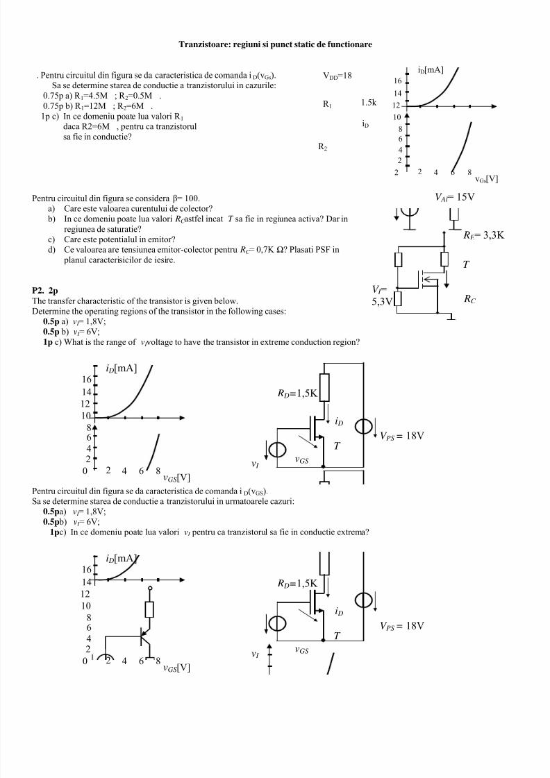
iD [mA]. Pentru circuitul din figura se da caracteristica de comanda iD(vGs). VDD=18Sa se determine starea de conductie a tranzistorului in cazurile:
0.75p a) R 1=4.5M ; R 2=0.5M .0.75p b) R 1=12M ; R 2=6M .1p c) In ce domeniu poate lua valori R 1
daca R2=6M , pentru ca tranzistorulsa fie in conductie?
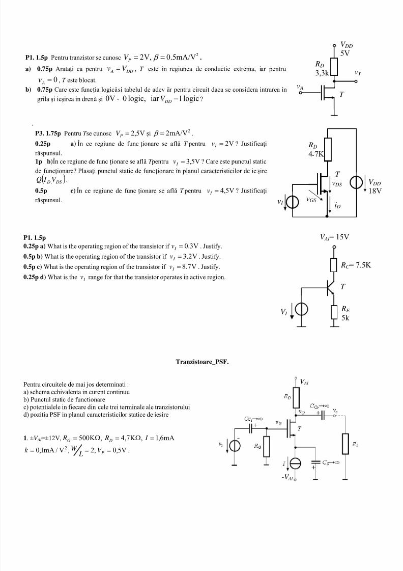
Pentru circuitul din figura se consideraβ = 100.a) Care este valoarea curentului de colector? b) In ce domeniu poate lua valori RC astfel incatT sa fie in regiunea activa? Dar in
regiunea de saturatie?c) Care este potentialul in emitor?d) Ce valoarea are tensiunea emitor-colector pentru RC = 0,7K Ω? Plasati PSF in
planul caracterisicilor de iesire.
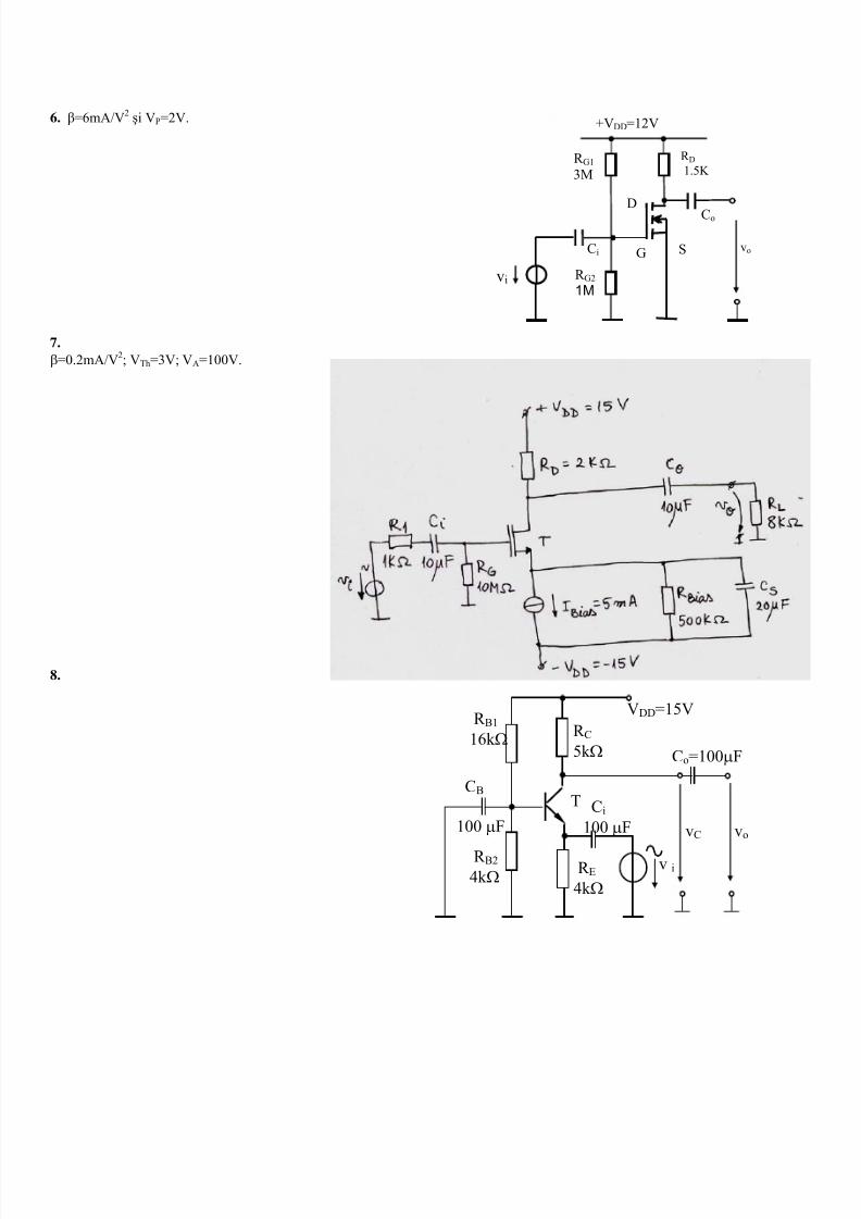
P2. 2pThe transfer characteristic of the transistor is given below.Determine the operating regions of the transistor in the following cases:
0.5p a) v I = 1,8V;0.5p b) v I = 6V;1p c) What is the range ofv I voltage to have the transistor in extreme conduction region?
Pentru circuitul din figura se da caracteristica de comanda iD(vGS).Sa se determine starea de conductie a tranzistorului in urmatoarele cazuri:
0.5p a) v I = 1,8V;0.5p b) v I = 6V;
1p c) In ce domeniu poate lua valoriv I pentru ca tranzistorul sa fie in conductie extrema?
R 1
R 2
1.5k
iD
6
16
12
2
10
14
8
4
2 4 6 82 vGs [V]
V Al = 15V
R E = 3,3K
T
V I =5,3V RC
V PS = 18V
v I
i D
T
R D= 1,5K
vGS
6
1210
14
2
16
2
8
4
4 6 80vGS [V]
i D [mA]
V PS = 18V
v I
i D
T
R D= 1,5K
vGS
6
12
2
10
1416
2 4 6 8v
8
4
0GS [V]
i D [mA]
7/21/2019 Dispozitive si circuite electronice
http://slidepdf.com/reader/full/dispozitive-si-circuite-electronice-56d9365157aa2 28/45
v A
vY
V DD 5V
R D
3,3k
T
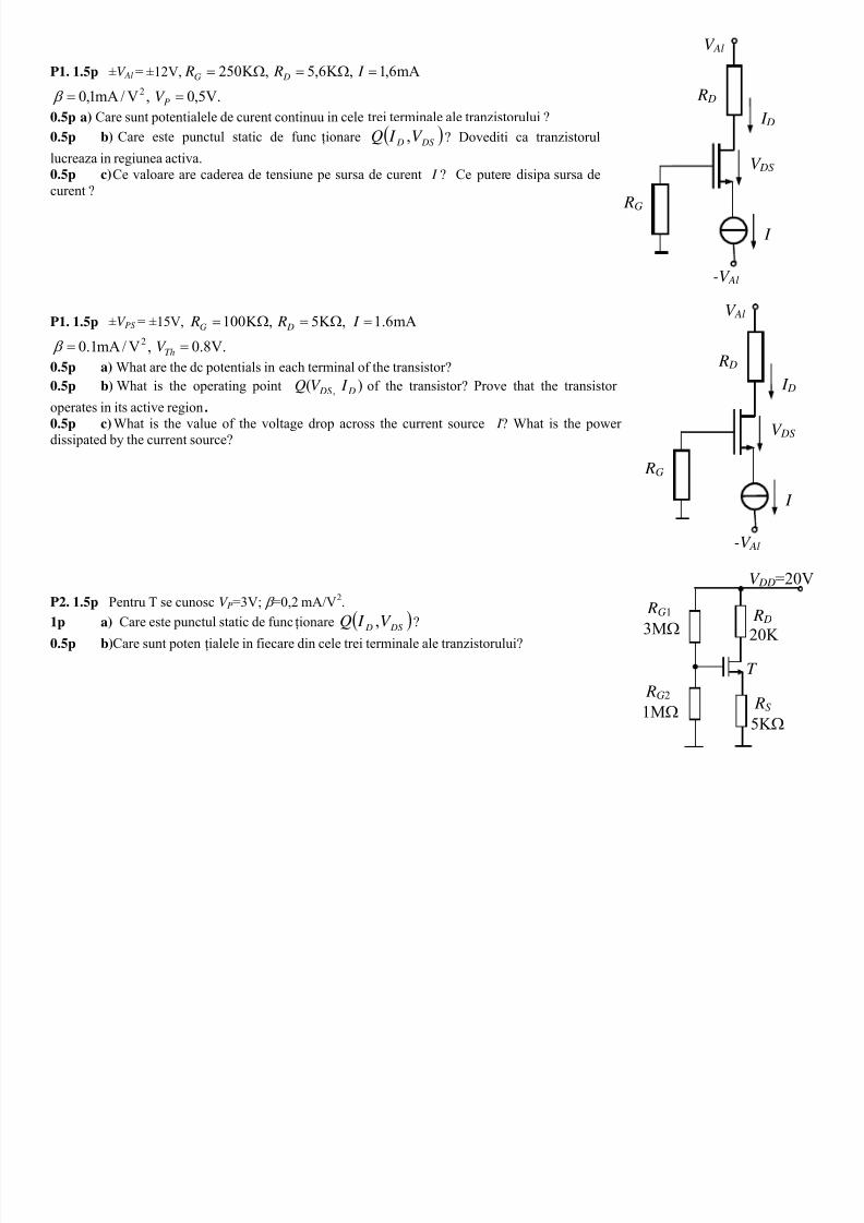
P1. 1.5p Pentru tranzistor se cunosc .20.5mA/VV,2 == β PV
a) 0.75p Arataţi ca pentru DD A V v = , T este in regiunea de conductie extrema, iar pentru0= Av , T este blocat.
b) 0.75p Care este funcţia logică si tabelul de adevăr pentru circuit daca se considera intrarea in
grilaşi ieşirea in drenă şi logic1iarlogic,0 -V0 − DDV ?
.P3. 1.75p PentruT se cunosc şi .V5,2=PV 2mA/V2= β
V DD
18v I i D
v DS
T
R D 4 7K
vGS
0.25p a) În ce regiune de funcţionare se află T pentru V2= I v ? Justificaţir ăspunsul.1p b) În ce regiune de funcţionare se află T pentru V5,3= I v ? Care este punctul staticde funcţionare? Plasaţi punctul static de funcţionare în planul caracteristicilor de ieşire
( ) DS D V I Q , .0.5p c) În ce regiune de funcţionare se află T pentru V5,4= I v ? Justificaţi
r ăspunsul.
V Al = 15V
RC = 7.5K
R E
5kV I
T
P1. 1.5p0.25p a) What is the operating region of the transistor if V3.0= I v . Justify.0.5p b) What is the operating region of the transistor if V2.3= I v . Justify.0.5p c) What is the operating region of the transistor if V7.8= I v . Justify.0.25p d) What is the range for that the transistor operates in active region. I v
Tranzistoare_PSF.
V Al
-V Al
Pentru circuitele de mai jos determinati :a) schema echivalenta in curent continuu
b) Punctul static de functionarec) potentialele in fiecare din cele trei terminale ale tranzistoruluid) pozitia PSF in planul caracteristicilor statice de iesire
1. ±V Al=±12V, mA6,1,K 7,4,K 500 =Ω=Ω= I R R DG
V5,0,2,V/mA1,0 2 === PV LW k .

7/21/2019 Dispozitive si circuite electronice
http://slidepdf.com/reader/full/dispozitive-si-circuite-electronice-56d9365157aa2 29/45
2. ,V12= AlV Ω=Ω=Ω== K 2,2,K 12,K 24,200 21 E B B R R R β Ω= K 2C R . Pentru tranzistorul T, VBE , on=0,6V V Al
iC
vO
3.For T: VTh=3V;β=0.1 mA/V2;.
4.Tranzistorul T are parametrii:β=0,2 mA/V2;VP=3V; VA=100V
5.
2 4 6 8
2
4
6
8
vCE
[V]
iB1=10μA
iB2=20μA
iB3=30μA
iB4=40μA
Pentru tranzistorul T, VBE , on=0,6V
R B1 10K Ω
R B2 5K Ω
T
R C 2K Ω
R L 3Κ Ω
CB=47μF
CC 47μ F
VCC=12V
vi R E 1,7K Ω
vOCΕ 47μF
7/21/2019 Dispozitive si circuite electronice
http://slidepdf.com/reader/full/dispozitive-si-circuite-electronice-56d9365157aa2 30/45
6. β=6mA/V2 şi VP=2V.
S vo
R D1.5K
R G1 3M
Co
vi R G21M
Ci
D
G
+VDD =12V
7.β=0.2mA/V2; VTh=3V; VA=100V.
8.
R B1 16k Ω
R B2 4k Ω
T
R C 5k Ω
R E 4k Ω
CB
100μF
Co=100μF
VDD=15V
vi
Ci 100μF vo vC
7/21/2019 Dispozitive si circuite electronice
http://slidepdf.com/reader/full/dispozitive-si-circuite-electronice-56d9365157aa2 31/45
I
RG
V DS
-V Al
R D
V Al
I D
P1. 1.5p ±V Al = ±12V, mA6,1,K 6,5,K 250 =Ω=Ω= I R R DG
V.5,0,V/mA1,0 2 == PV β 0.5p a) Care sunt potentialele de curent continuu in cele trei terminale ale tranzistorului ? 0.5p b) Care este punctul static de funcţionare ( ) DS D V I Q , ? Dovediti ca tranzistorullucreaza in regiunea activa.0.5p c) Ce valoare are caderea de tensiune pe sursa de curent I ? Ce putere disipa sursa decurent ?
I
RG
V DS
-V Al
R D
V Al
I D
P1. 1.5p ±V PS = ±15V, mA6.1,K 5,K 100 =Ω=Ω= I R R DG
V.8.0,V/mA1.0 2 == ThV β 0.5p a) What are the dc potentials in each terminal of the transistor?0.5p b) What is the operating point of the transistor? Prove that the transistoroperates in its active region.
)( , D DS I V Q
0.5p c) What is the value of the voltage drop across the current source I ? What is the powerdissipated by the current source?
RG1 3MΩ
RG2 1MΩ
T
R D
20K
RS 5K Ω
V DD =20V P2. 1.5p Pentru T se cunoscV P=3V; β =0,2 mA/V2. 1p a) Care este punctul static de funcţionare ( ) DS D V I Q , ?
0.5p b) Care sunt potenţialele in fiecare din cele trei terminale ale tranzistorului?
7/21/2019 Dispozitive si circuite electronice
http://slidepdf.com/reader/full/dispozitive-si-circuite-electronice-56d9365157aa2 32/45
Tranzistoare MOS in comutare
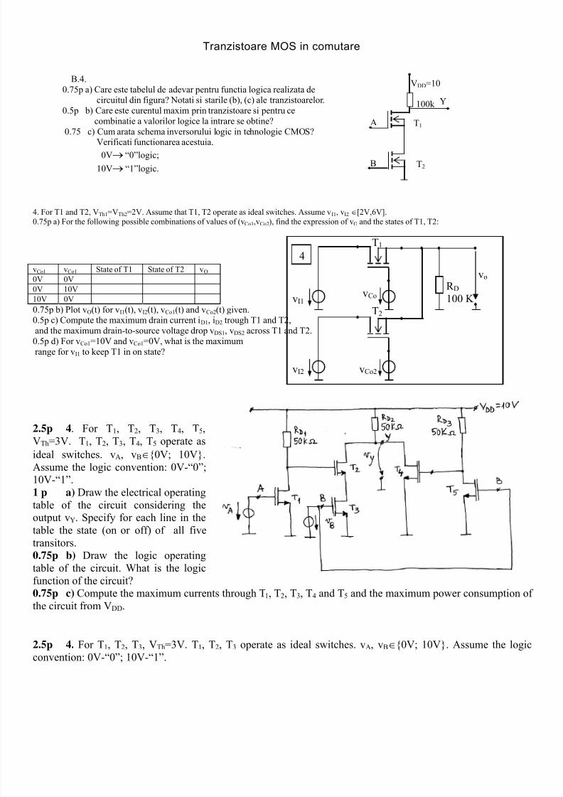
B.4. VDD=100.75p a) Care este tabelul de adevar pentru functia logica realizata de
circuitul din figura? Notati si starile (b), (c) ale tranzistoarelor. Y100k0.5p b) Care este curentul maxim prin tranzistoare si pentru ce
combinatie a valorilor logice la intrare se obtine? A T1
T2
0.75 c) Cum arata schema inversorului logic in tehnologie CMOS?Verificati functionarea acestuia.
0V→ “0”logic;B10V → “1”logic.
4. For T1 and T2, V Th1=V Th2=2V. Assume that T1, T2 operate as ideal switches. Assume v I1, v I2 ∈ [2V,6V].0.75p a) For the following possible combinations of values of (v Co1 ,vCo2), find the expression of v O and the states of T1, T2:
R D100 K vCovI1
vCo2
T1
T2
vI2
vo vCo1 vCo1 State of T1 State of T2 v O
0V 0V0V 10V10V 0V0.75p b) Plot v O(t) for v I1(t), v I2(t), v Co1(t) and v Co2(t) given.0.5p c) Compute the maximum drain current i D1, iD2 trough T1 and T2,and the maximum drain-to-source voltage drop v DS1 , vDS2 across T1 and T2.
4
0.5p d) For v Co1 =10V and v Co1=0V, what is the maximumrange for v I1 to keep T1 in on state?
2.5p 4 . For T 1, T2, T3, T4, T5,VTh=3V. T 1, T2, T3, T4, T5 operate asideal switches. v A, vB∈ 0V; 10V.Assume the logic convention: 0V-“0”;10V-“1”.1 p a) Draw the electrical operatingtable of the circuit considering theoutput v Y. Specify for each line in thetable the state (on or off) of all fivetransitors.
0.75p b) Draw the logic operatingtable of the circuit. What is the logicfunction of the circuit?0.75p c) Compute the maximum currents through T 1, T2, T3, T 4 and T 5 and the maximum power consumption ofthe circuit from V DD .
2.5p 4. For T 1, T2, T3, V Th=3V. T 1, T2, T3 operate as ideal switches. v A, vB∈ 0V; 10V. Assume the logicconvention: 0V-“0”; 10V-“1”.

7/21/2019 Dispozitive si circuite electronice
http://slidepdf.com/reader/full/dispozitive-si-circuite-electronice-56d9365157aa2 33/45
1p a) Draw the electrical operating table of the circuitfor all the possible voltage combinations of v A, v B. Specifyfor each line in the table the state (on or off) of T 1, T 2 andT3.0.5p b) Draw the logic operating table of the circuit.What is the logic function of the circuit?0.5p c) Compute the maximum power consumption of
the circuit from V DD . For what combinations of values of v A and v B does this maximum power consumption appear?0.5p d) Sketch the CMOS implementation of the samecircuit. What would be the advantage of CMOSimplementation as compared to the one given above?
P3. 2.5p For T, its parameters are: β=0.125mA/V 2; V Th=2V.
Assume v Co∈
0V; 10V. Assume that forthese two values of v Co , T can only operate in (off) and (ex.c.) states.Assume v I∈ [1V; 5V].
a) 1p Proove that, for v Co∈ 0V; 10Vand v I∈ [1V; 5V], T can only operatein (off) and (ex.c.) states. Which ofthe two values of v Co will bring T in: (1) (off) state; (2) (ex.c.) state?
vCo vO
vI
T
R L56 K
G
SD
b) 0.5p Find the expression v O(v I, vCo) for v Co∈ 0V; 10V and v I∈ [1V; 5V], using for T in (off) and (ex.c.) states, theideal switch model. For each value of v Co, draw the VTC v O(v I) of the circuit.
c) 0.75p Draw v O(t) for v I(t) and v Co(t) below. What is the application of the circuit? d) 0.25p Find the maximum possible value of v I for which, at v Co=10V, T operates in (ex.c.) state.
21
3
0t
vI [V]
4
5
10
0t
vCo [V]

7/21/2019 Dispozitive si circuite electronice
http://slidepdf.com/reader/full/dispozitive-si-circuite-electronice-56d9365157aa2 34/45
v A
vY
V DD 5V
R D
3,3k
T
P1. 1.5p Pentru tranzistor se cunosc .20.5mA/VV,2 == β PV
a) 0.75p Arata ţi ca pentru DD A V v = , T este in regiunea de conductie extrema,iar pentru 0=
Av , T este blocat.b) 0.75p Care este func ţia logic ă si tabelul de adev ăr pentru circuit daca se
considera intrarea in grila şi ie şirea in dren ă şi logic1 ? iarlogic,0 -V0 −
DDV
P.3 . 2.5pPentru tranzistoarele T ni, V Pn=3V iar pentrutranzistoarele T pi, VPp= -3V. Toatetranzistoarele lucreaza ca intrerupatoareideale. v A, vB∈ 0V; 10V. Se consideraconventia logica: 0V-“0”; 10V-“1”. 1.25p a) Completati tabelul de functionareelectrica a circuitului, precizand atat valoarea
tensiunii de iesire v Y’ cat si a tensiunii deiesire v Y. Pentru fiecare linie din tabel, precizati starea fiecarui tranzistor din schema((b) sau (c.ex.)).
T n1
T n2
T p2
'Y
A
B
V DD =10V
T p1 T p3
T n3
Y
v B
v y’
v y
0.75p b) Cum arata tabelul de functionarelogica a circuitului cu iesirea Y’ ? Ce functielogica realizeaza circuitul cu iesirea Y’?0.5p c) Cum arata tabelul de functionare logica a circuitului cu iesirea Y ? Ce functie logica realizeaza circuitulcu iesirea Y ?

7/21/2019 Dispozitive si circuite electronice
http://slidepdf.com/reader/full/dispozitive-si-circuite-electronice-56d9365157aa2 35/45
Amplificatoare cu T
1. Pentru amplificatorul din figura se cunosc:±V Al=±12V, mA6,1,K 7,4,K 500 =Ω=Ω= I R R DG
V5,0,2,V/mA1,0 2 === PV LW k .
a) 0,75p . Care este PSF ?( ) DS D V I ,
b) 0,75p. Ce valori au parametrii amplificatorului oiv R R A ,, ? Careeste modelul echivalent al amplificatorului?c) 0,75p . Care sunt cronogramele semnalelor
),(), pentru ]mV[(),(),( t it vt vt v DOoG sin500)( t t vi ω = ?
-V Al
V Al
d) 0,75p. In ce conexiune este amplificatorul ? Care parametri aiamplificatorului se modifica si cum daca la iesire se conecteaza orezistenta de sarcina ? K 7,4 Ω= L R
1.Pentru amplificatorul din figura se cunosc: V12= AlV ,Ω=Ω=Ω== K 2,2,K 12,K 24,200 21 E B B R R R β
iC
V Al
vO
Ω= K 2C R .e) 0,75p . Care este PSF ?( )CE C V I ,f) 0,75p. Ce valori au parametrii de semnal mic ai tranzistorului ? Care este
schema echivalenta pentru variatii a amplificatorului ?. Se consider ă mA5,1= .C I
g) 0,75p . In ce conexiune este amplificatorul ? Ce valori au oiv R R ? A ,,h) 0,75p. Care sunt cronogramele semnalelor ),(), pentru
]mV[(),( t it vt v C Oo
sin20)( t t vi ω = ?
P1. 2.5pFor T: VTh=3V;β=0.1 mA/V2; VA=100V.a) 0.75p Draw the D.C. equivalent circuit for this schematic. Compute the quiescent point of T, Q(VDS, ID), and show that T is biain (a F).b) 0.75p Compute the D.C. voltage drops onall the components in the circuit above(including the capacitors).c) 0.5p Compute the following small signalmodel parameters of T: gm; r o. Does thetransistor model and/or the model parametersmodify if we use a transistor with the sameβ and VA, but with VTh=4V? Explain youranswer.d) 0.5p Draw the small signal equivalentcircuit of this stage in midfrequency. What is
the configuration of this stage and what is thevalue of the voltage gain Av=
i
ovv ? (You can
assume r o sufficiently large to be ignored in thecomputation).
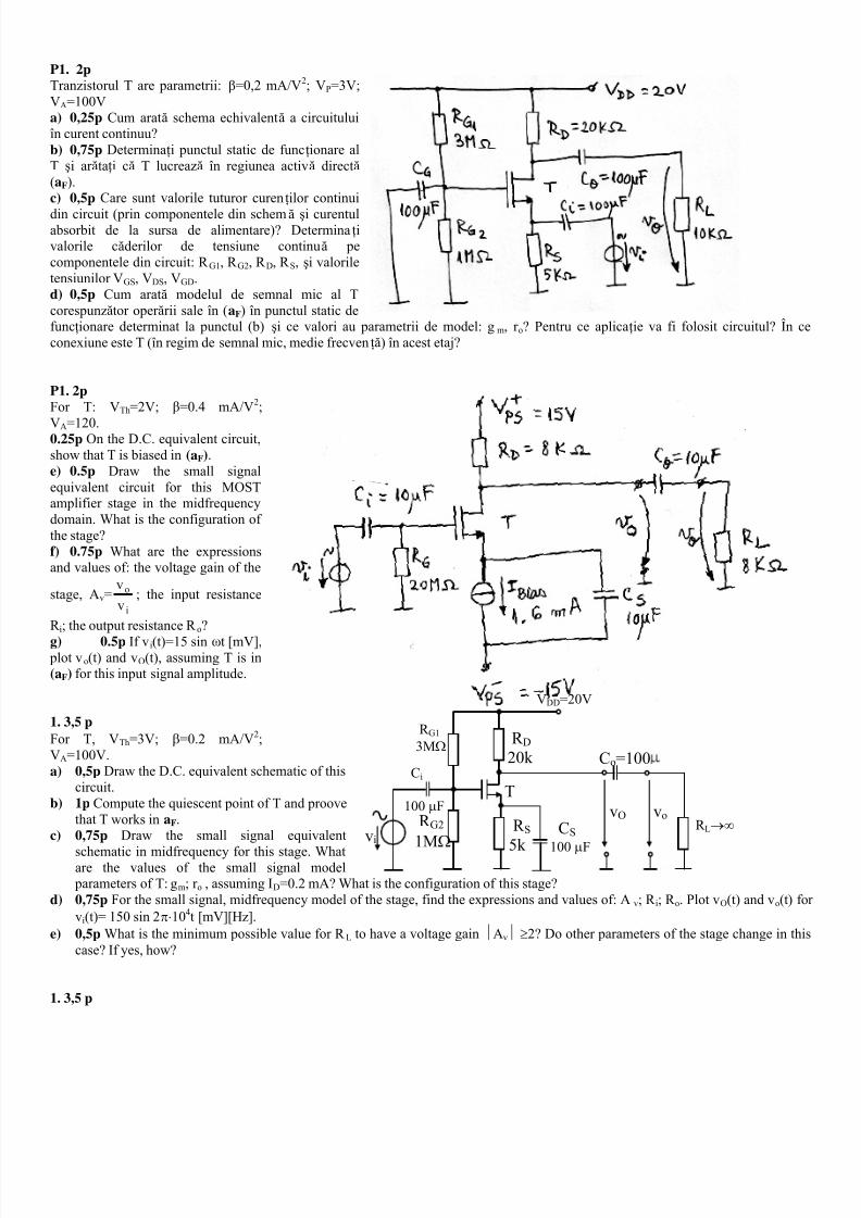
7/21/2019 Dispozitive si circuite electronice
http://slidepdf.com/reader/full/dispozitive-si-circuite-electronice-56d9365157aa2 36/45
P1. 2pTranzistorul T are parametrii:β=0,2 mA/V2; VP=3V;VA=100Va) 0,25p Cum arată schema echivalentă a circuituluiîn curent continuu?b) 0,75p Determinaţi punctul static de funcţionare alT şi ar ătaţi că T lucrează în regiunea activă directă (a F). c) 0,5p Care sunt valorile tuturor curenţilor continuidin circuit (prin componentele din schemă şi curentulabsorbit de la sursa de alimentare)? Determinaţivalorile căderilor de tensiune continuă pecomponentele din circuit: R G1, R G2, R D, R S, şi valoriletensiunilor VGS, VDS, VGD.d) 0,5p Cum arată modelul de semnal mic al Tcorespunzător oper ării sale în (a F) în punctul static defuncţionare determinat la punctul (b)şi ce valori au parametrii de model: gm, r o? Pentru ce aplicaţie va fi folosit circuitul? Înconexiune este T (în regim de semnal mic, medie frecvenţă) în acest etaj?
P1. 2pFor T: VTh=2V; β=0.4 mA/V2;
VA=120.0.25p On the D.C. equivalent circuit,show that T is biased in(a F).e) 0.5p Draw the small signalequivalent circuit for this MOSTamplifier stage in the midfrequencydomain. What is the configuration ofthe stage?f) 0.75p What are the expressionsand values of: the voltage gain of the
stage, Av=i
ovv ; the input resistance
R i; the output resistance R o? g) 0.5p If vi(t)=15 sinωt [mV], plot vo(t) and vO(t), assuming T is in(a F) for this input signal amplitude.
1. 3,5 pFor T, VTh=3V; β=0.2 mA/V2;VA=100V.a) 0,5p Draw the D.C. equivalent schematic of this
circuit.b) 1p Compute the quiescent point of T and proove
that T works ina F.c) 0,75p Draw the small signal equivalent
schematic in midfrequency for this stage. Whatare the values of the small signal model parameters of T: gm; r o , assuming ID=0.2 mA? What is the configuration of this stage?
VDD=20V
R G1 3MΩ
R G2 1MΩ
T
R D 20k
R S
5k
Ci
100μF
Co=100
vi CS
100μF
vo vO R L→∞
d) 0,75p For the small signal, midfrequency model of the stage, find the expressions and values of: Av; R i; R o. Plot vO(t) and vo(t) fovi(t)= 150 sin 2π⋅104t [mV][Hz].
e) 0,5p What is the minimum possible value for R L to have a voltage gain Av ≥2? Do other parameters of the stage change incase? If yes, how?
1. 3,5 p
7/21/2019 Dispozitive si circuite electronice
http://slidepdf.com/reader/full/dispozitive-si-circuite-electronice-56d9365157aa2 37/45
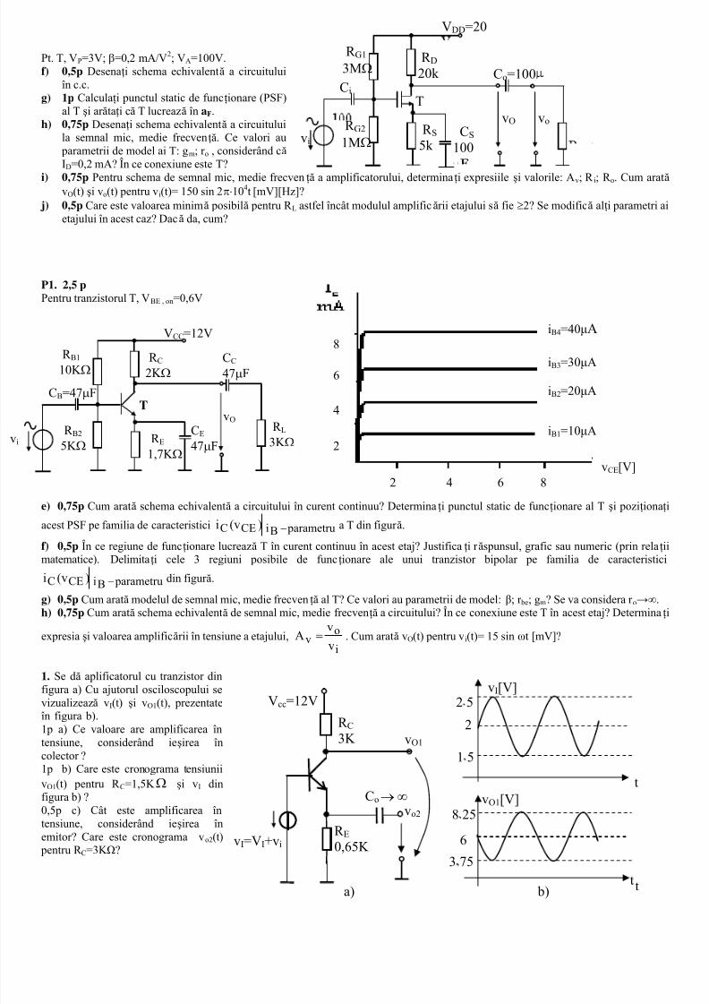
VDD=20
R G1 Pt. T, VP=3V;β=0,2 mA/V2; VA=100V.3MΩf) 0,5p Desenaţi schema echivalentă a circuitului
în c.c.g) 1p Calculaţi punctul static de funcţionare (PSF)
al Tşi ar ătaţi că T lucrează în a F.h) 0,75p Desenaţi schema echivalentă a circuitului
la semnal mic, medie frecvenţă. Ce valori au parametrii de model ai T: gm; r o , considerând că ID=0,2 mA? În ce conexiune este T?
i) 0,75p Pentru schema de semnal mic, medie frecvenţă a amplificatorului, determinaţi expresiileşi valorile: Av; R i; R o. Cum aravO(t) şi vo(t) pentru vi(t)= 150 sin 2π⋅104t [mV][Hz]?
j) 0,5p Care este valoarea minimă posibilă pentru R L astfel încât modulul amplificării etajului să fie ≥2? Se modifică alţi parametri etajului în acest caz? Dacă da, cum?
P1. 2,5 pPentru tranzistorul T, VBE , on=0,6V
e) 0,75p Cum arată schema echivalentă a circuitului în curent continuu? Determinaţi punctul static de funcţionare al Tşi poziţiona
acest PSF pe familia de caracteristici parametruBiCEC )(vi − a T din figur ă.f) 0,5p În ce regiune de funcţionare lucrează T în curent continuu în acest etaj? Justificaţi r ăspunsul, grafic sau numeric (prin reţmatematice). Delimitaţi cele 3 regiuni posibile de funcţionare ale unui tranzistor bipolar pe familia de caracte
parametruBiCEC )(vi − din figur ă.
g) 0,5p Cum arată modelul de semnal mic, medie frecvenţă al T? Ce valori au parametrii de model:β; r be; gm? Se va considera r o→∞ . h) 0,75p Cum arată schema echivalentă de semnal mic, medie frecvenţă a circuitului? În ce conexiune este T în acest etaj? Deter
expresiaşi valoarea amplificării în tensiune a etajului,io
v vvA = . Cum arată vO(t) pentru vi(t)= 15 sinωt [mV]?
1. Se dă aplificatorul cu tranzistor dinfigura a) Cu ajutorul osciloscopului se
vizualizează vI(t) şi vO1(t), prezentateîn figura b). 1p a) Ce valoare are amplificarea întensiune, considerând ieşirea încolector ?1p b) Care este cronograma tensiuniivO1(t) pentru R C=1,5K Ω şi vI dinfigura b) ?0,5p c) Cât este amplificarea întensiune, considerând ieşirea înemitor? Care este cronograma vo2(t) pentru R C=3K Ω?
R G2 1MΩ
T
R D 20k
R S5k
CiC =100o
vi CS 100
vO vo
R B1 10K Ω
R B2 5K Ω
T
R C 2K Ω
R L 3Κ Ω
CB=47μF
CC 47μF
VCC=12V
R E 1,7K Ω
CΕ 47μF
vO
2 4 6 8
2
4
6
8
vCE[V]
iB1=10μA
iB2=20μA
iB3=30μA
iB4=40μA
t
vI[V]
22
vo2
vI=VI+vi
vO1
R C 3K
Co ∞→
R E 0,65K
Vcc=12V 5
t
vO1[V]
63 75
1 5
8 25
t a) b)
7/21/2019 Dispozitive si circuite electronice
http://slidepdf.com/reader/full/dispozitive-si-circuite-electronice-56d9365157aa2 38/45
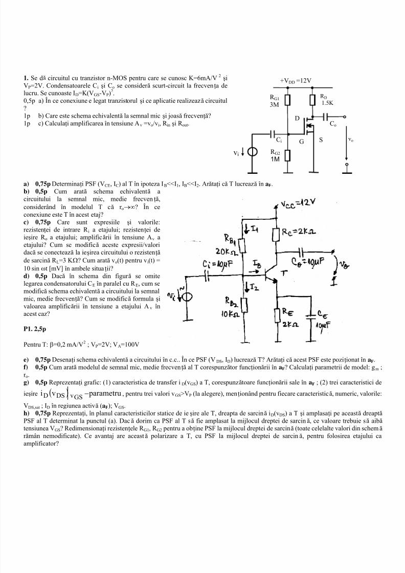
1. Se dă circuitul cu tranzistor n-MOS pentru care se cunosc K=6mA/V2 şiVP=2V. Condensatoarele Ci şi Co se consider ă scurt-circuit la frecvenţa delucru. Se cunoaste ID=K(VGS-VP)2.
S vo
R D1.5K R G1 3M
Co
vi R G21M
Ci
D
G
+VDD =12V
0,5p a) În ce conexiune e legat tranzistorulşi ce aplicatie realizează circuitul?1p b) Care este schema echivalentă la semnal micşi joasă frecvenţă?1p c) Calculaţi amplificarea în tensiune Av =vo/vi, R in şi R out.
a) 0,75p Determinaţi PSF (VCE, IC) al T în ipoteza IB<<I1, IB<<I2. Ar ătaţi că T lucrează în aF.b) 0,5p Cum arată schema echivalentă a
circuitului la semnal mic, medie frecvenţă,considerând în modelul T că r o→∞? În ceconexiune este T în acest etaj? c) 0,75p Care sunt expresiile şi valorile:rezistenţei de intrare R i a etajului; rezistenţei deieşire R o a etajului; amplificării în tensiune Av aetajului? Cum se modifică aceste expresii/valoridacă se conectează la ieşirea circuitului o rezistenţă de sarcină R L=3 K Ω? Cum arată vo(t) pentru vi(t) =10 sinωt [mV] în ambele situaţii? d) 0,5p Dacă în schema din figur ă se omitelegarea condensatorului CE în paralel cu R E, cum semodifică schema echivalentă a circuitului la semnal
mic, medie frecvenţă? Cum se modifică formulaşivaloarea amplificării în tensiune a etajului Av înacest caz?
P1. 2,5p
Pentru T:β=0,2 mA/V2 ; VP=2V; VA=100V
e) 0,75p Desenaţi schema echivalentă a circuitului în c.c.. În ce PSF (VDS, ID) lucrează T? Ar ătaţi că acest PSF este poziţionat înaF.f) 0,5p Cum arată modelul de semnal mic, medie frecvenţă al T corespunzător funcţionării îna F? Calculaţi parametrii de model: gmr o.g) 0,5p Reprezentaţi grafic: (1) caracteristica de transfer iD(vGS) a T, corespunzătoare funcţionării sale îna F ; (2) trei caracteristiciieşire ( ) parametruvi GSvDSD − , pentru trei valori vGS>VP (la alegere), menţionând pentru fiecare caracteristică, numeric, valori
VDS,sat ; ID în regiunea activă (a F); VGS. h) 0,75p Reprezentaţi, în planul caracteristicilor statice de ieşire ale T, dreapta de sarcină iD(vDS) a T şi amplasaţi pe această dreapPSF al T determinat la punctul (a). Dacă dorim ca PSF al T să fie amplasat la mijlocul dreptei de sarcină, ce valoare trebuie să aibtensiunea VGS? Redimensionaţi rezistenţele R G1, R G2 pentru a obţine PSF la mijlocul dreptei de sarcină (toate celelalte valori din scher ămân nemodificate). Ce avantaj are această polarizare a T, cu PSF la mijlocul dreptei de sarcină, pentru folosirea etajuluiamplificator?
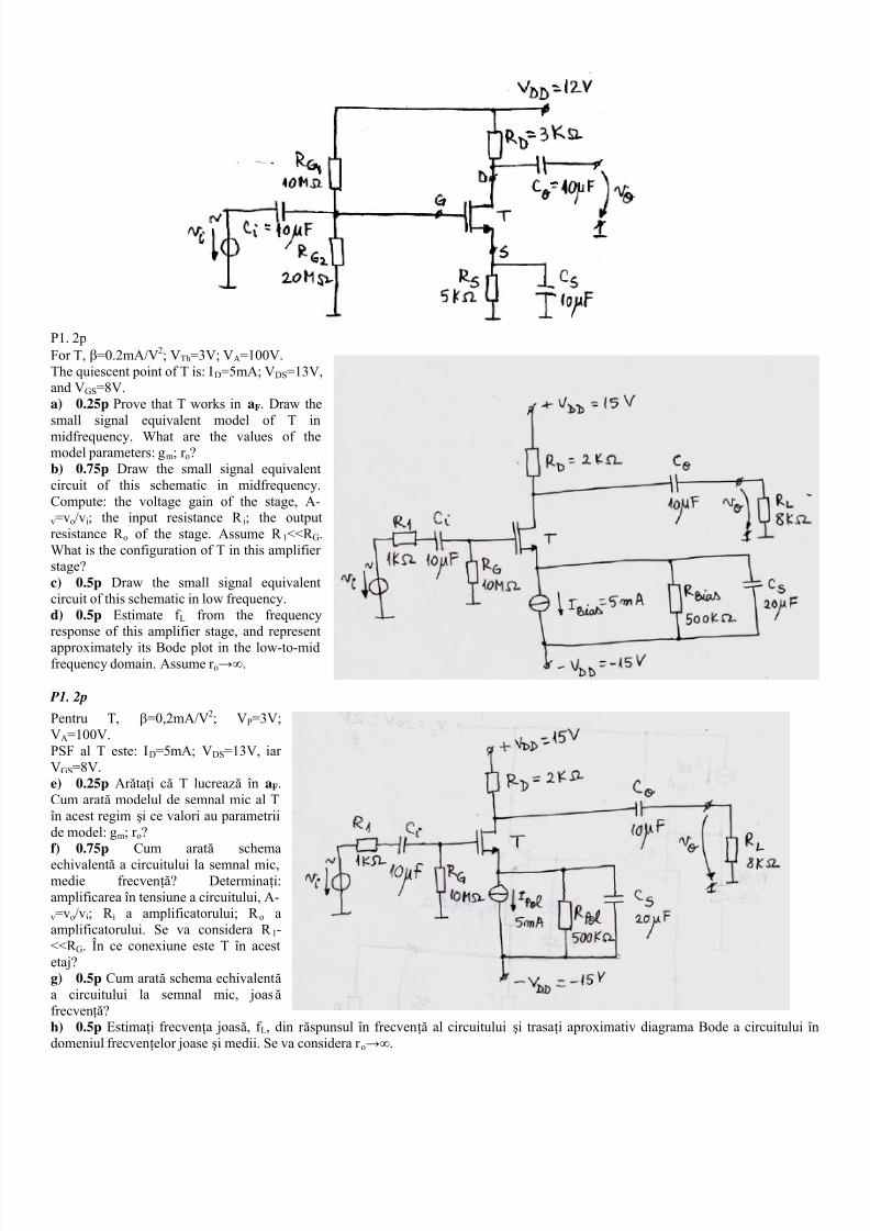
7/21/2019 Dispozitive si circuite electronice
http://slidepdf.com/reader/full/dispozitive-si-circuite-electronice-56d9365157aa2 39/45
P1. 2pFor T,β=0.2mA/V2; VTh=3V; VA=100V.The quiescent point of T is: ID=5mA; VDS=13V,and VGS=8V.a) 0.25p Prove that T works ina F. Draw thesmall signal equivalent model of T inmidfrequency. What are the values of themodel parameters: gm; r o?b) 0.75p Draw the small signal equivalentcircuit of this schematic in midfrequency.Compute: the voltage gain of the stage, A-v=vo/vi; the input resistance R i; the outputresistance R o of the stage. Assume R 1<<R G.What is the configuration of T in this amplifierstage? c) 0.5p Draw the small signal equivalentcircuit of this schematic in low frequency. d) 0.5p Estimate f L from the frequencyresponse of this amplifier stage, and representapproximately its Bode plot in the low-to-midfrequency domain. Assume r o→∞ .
P1. 2p
Pentru T, β=0,2mA/V2; VP=3V;VA=100V.PSF al T este: ID=5mA; VDS=13V, iarVGS=8V.e) 0.25p Ar ătaţi că T lucrează în a F.Cum arată modelul de semnal mic al Tîn acest regimşi ce valori au parametriide model: gm; r o?f) 0.75p Cum arată schemaechivalentă a circuitului la semnal mic,medie frecvenţă? Determinaţi:amplificarea în tensiune a circuitului, A-v=vo/vi; R i a amplificatorului; R o aamplificatorului. Se va considera R 1-<<R G. În ce conexiune este T în acestetaj? g) 0.5p Cum arată schema echivalentă a circuitului la semnal mic, joasă frecvenţă? h) 0.5p Estimaţi frecvenţa joasă, f L, din r ăspunsul în frecvenţă al circuituluişi trasaţi aproximativ diagrama Bode a circuituldomeniul frecvenţelor joaseşi medii. Se va considera r o→∞ .
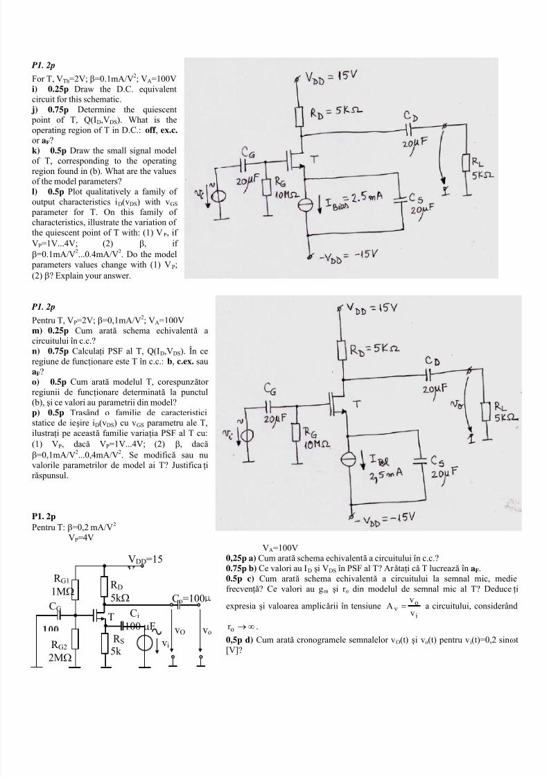
7/21/2019 Dispozitive si circuite electronice
http://slidepdf.com/reader/full/dispozitive-si-circuite-electronice-56d9365157aa2 40/45
P1. 2p
For T, VTh=2V;β=0.1mA/V2; VA=100Vi) 0.25p Draw the D.C. equivalentcircuit for this schematic.
j) 0.75p Determine the quiescent point of T, Q(ID,VDS). What is theoperating region of T in D.C.:off , ex.c. or a F? k) 0.5p Draw the small signal modelof T, corresponding to the operatingregion found in (b). What are the valuesof the model parameters? l) 0.5p Plot qualitatively a family ofoutput characteristics iD(vDS) with vGS parameter for T. On this family ofcharacteristics, illustrate the variation ofthe quiescent point of T with: (1) VP, ifVP=1V...4V; (2) β, ifβ=0.1mA/V2...0.4mA/V2. Do the model parameters values change with (1) VP;(2)β? Explain your answer.
P1. 2p
Pentru T, VP=2V;β=0,1mA/V2; VA=100Vm) 0.25p Cum arată schema echivalentă acircuitului în c.c.?n) 0.75p Calculaţi PSF al T, Q(ID,VDS). În ceregiune de funcţionare este T în c.c.:b , c.ex. saua F? o) 0.5p Cum arată modelul T, corespunzătorregiunii de funcţionare determinată la punctul(b),şi ce valori au parametrii din model? p) 0.5p Trasând o familie de caracteristicistatice de ieşire iD(vDS) cu vGS parametru ale T,ilustraţi pe această familie variaţia PSF al T cu:(1) VP, dacă VP=1V...4V; (2) β, dacă β=0,1mA/V2...0,4mA/V2. Se modifică sau nuvalorile parametrilor de model ai T? Justificaţir ăspunsul.
P1. 2pPentru T:β=0,2 mA/V2
VP=4VVA=100V
0,25p a) Cum arată schema echivalentă a circuitului în c.c.?0.75p b) Ce valori au ID şi VDS în PSF al T? Ar ătaţi că T lucrează în a F.
VDD=15
R G1 1MΩ
R G2 2MΩ
T
R D 5
0.5p c) Cum arată schema echivalentă a circuitului la semnal mic, mefrecvenţă? Ce valori au gm şi r o din modelul de semnal mic al T? Dedu
expresiaşi valoarea amplicării în tensiunei
ov v
vA = a circuitului, considerâ
∞→or .
k Ω
R S 5k
CGC =100o
0,5p d) Cum arată cronogramele semnalelor vO(t) şi vo(t) pentru vi(t)=0,2 sinω[V]?
vi
Ci 100μF vO vo
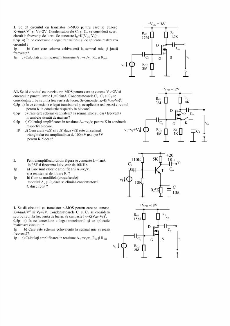
7/21/2019 Dispozitive si circuite electronice
http://slidepdf.com/reader/full/dispozitive-si-circuite-electronice-56d9365157aa2 41/45
S vo
R D1.5K
R G1 15M
Co
vi R G23M
Ci
D
G
+VDD =18V1. Se dă circuitul cu tranzistor n-MOS pentru care se cunoscK=6mA/V2 şi VP=2V. Condensatoarele Ci şi Co se consider ă scurt-circuit la frecvenţa de lucru. Se cunoaste ID=K(VGS-VP)2.0,5p a) În ce conexiune e legat tranzistorulşi ce aplicatie realizează circuitul ?1p b) Care este schema echivalentă la semnal micşi joasă frecvenţă?1p c) Calculaţi amplificarea în tensiune Av =vo/vi, R in şi R out.
A1. Se dă circuitul cu tranzistor n-MOS pentru care se cunosc VP=2V sicurentul in punctul static ID=0.5mA. Condensatoarele Ci , Co si CS seconsider ă scurt-circuit la frecvenţa de lucru. Se cunoaste ID=K(VGS-VP)2.0,5p a) În ce conexiune e legat tranzistorulşi ce aplicatie realizează circuitul
pentru K in conductie respectiv in blocare?
0.5p b) Care este schema echivalentă la semnal micşi joasă frecvenţă in ambele situatii de mai sus?0.5p c) Calculaţi amplificarea în tensiune Av =vo/vi pentru K in conductie vo
R D6K
R G1 3M
Co
vI=vi+VI R G21M
Ci
D
G
+VDD =12V
R S1K
K
CS
vO
respectiv blocare.1P d) Cum arata vO(t) si vo(t) daca vI(t) este un semnal
triunghiular cu amplitudinea de 100mV axat pe 3V pentru K blocat ?
110K 5K
10K vi
+20
Ci
10~ Co
vo
0.5K 10
T
C
I. Pentru amplificatorul din figura se cunoaste IC=1mAin PSF si frecventa lui vi este de 10KHz.
1p a) Care sunt valorile amplificării Av=vo/vişi a rezistenţei de intrare R i ?
1p b) Cum se modifică (creşte/scade)modulul Av şi R i dacă se elimină condensatorulC din circuit ?
S vo
R D1.5K
R G1 15M
Co
vi R G23M
Ci
D
G
+VDD =18V1. Se dă circuitul cu tranzistor n-MOS pentru care se cunoscK=6mA/V2 şi VP=2V. Condensatoarele Ci şi Co se consider ă scurt-circuit la frecvenţa de lucru. Se cunoaste ID=K(VGS-VP)2.0,5p a) În ce conexiune e legat tranzistorulşi ce aplicatierealizează circuitul ?1p b) Care este schema echivalentă la semnal micşi joasă frecvenţă?1p c) Calculaţi amplificarea în tensiune Av =vo/vi, R in şi R out.
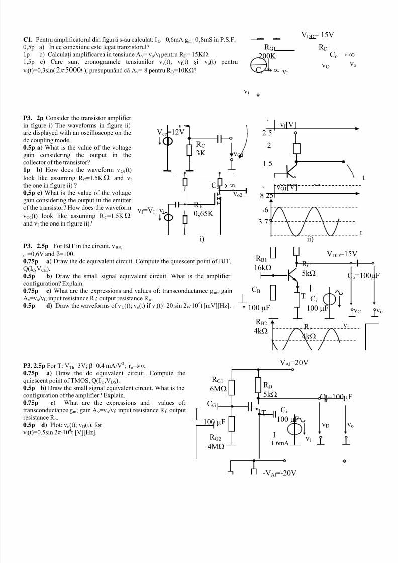
7/21/2019 Dispozitive si circuite electronice
http://slidepdf.com/reader/full/dispozitive-si-circuite-electronice-56d9365157aa2 42/45
Ci → ∞ vO vo Co → ∞
R G1 R D200K
VDD= 15V
vI
vi
C1. Pentru amplificatorul din figur ă s-au calculat: ID= 0,6mA gm=0,8mS în P.S.F.0,5p a) În ce conexiune este legat tranzistorul?1p b) Calculaţi amplificarea în tensiune Av= vo/vi pentru R D= 15K Ω.1,5p c) Care sunt cronogramele tensiunilor vi(t), vI(t) şi vo(t) pentruvi(t)=0,3sin( t 50002π ), presupunând că Av=-8 pentru R D=10K Ω?
P3. 2p Consider the transistor amplifierin figure i) The waveforms in figure ii)are displayed with an oscilloscope on thedc coupling mode.0.5p a) What is the value of the voltagegain considering the output in thecollector of the transistor?
vo2
vI=VI+vi
vO1
R C 3K
Co ∞→
R E 0,65K
Vcc=12V
t
vI[V]
22 5
t
vO1[V]
63 75
1 5
8 25
i) ii)
1p b) How does the waveform vO1(t)look like assuming R C=1.5K and vI the one in figure ii) ?
Ω
0,5p c) What is the value of the voltagegain considering the output in the emitterof the transistor? How does the waveformvO2(t) look like assuming R C=1.5K Ω and vI the one in figure ii)?
P3. 2.5p For BJT in the circuit, vBE,
on=0,6V andβ=100. R B1 16k Ω
R B2 4k Ω
T
R C 5k Ω
R E 4k Ω
CB
100μF
Co=100
VDD=15V
vi
Ci 100μF vC
0.75p a) Draw the dc equivalent circuit. Compute the quiescent point of BJT,Q(IC,VCE).0.5p b) Draw the small signal equivalent circuit. What is the amplifierconfiguration? Explain.0.75p c) What are the expressions and values of: transconductance gm; gainAv=vo/vi; input resistance R i; output resistance R o.0.5p d) Draw the waveforms of vC(t); vo(t) if vi(t)=20 sin 2π·104t [mV][Hz].
P3. 2.5p For T: VTh=3V;β=0.4 mA/V2; r o→∞.0.75p a) Draw the dc equivalent circuit. Compute thequiescent point of TMOS, Q(ID,VDS). R G1
6MΩ
R G2 4MΩ
T
R D
5k Ω
I1.6mA
CG
100μF
Co=1000.5p b) Draw the small signal equivalent circuit. What is theconfiguration of the amplifier? Explain. μF
VAl=20V
0.75p c) What are the expressions and values of:transconductance gm; gain Av=vo/vi; input resistance R i; outputresistance R o.0.5p d) Plot: vo(t); vD(t), forvi(t)=0.5sin 2π·104t [V][Hz].
vi
Ci 100μF vD vo
-VAl=-20V

7/21/2019 Dispozitive si circuite electronice
http://slidepdf.com/reader/full/dispozitive-si-circuite-electronice-56d9365157aa2 43/45
P.3. 2,5p
i) 0,75p Determinaţi PSF (VCE, IC) al T în ipotezaIB<<I1, IB<<I2. Ar ătaţi că T lucrează în a F.
j) 0,5p Cum arată schema echivalentă a circuituluila semnal mic, medie frecvenţă, considerând înmodelul T că r o→∞? În ce conexiune este T în acestetaj? k) 0,75p Care sunt expresiileşi valorile: rezistenţeide intrare R i a etajului; rezistenţei de ieşire R o aetajului; amplificării în tensiune Av a etajului? Cumse modifică aceste expresii/valori dacă se conectează la ieşirea circuitului o rezistenţă de sarcină R L=3K Ω? Cum arată vo(t) pentru vi(t) = 10 sinωt [mV] înambele situaţii? l) 0,5p Dacă în schema din figur ă se omite legareacondensatorului CE în paralel cu R E, cum se modifică schema echivalentă a circuitului la semnal mic,medie frecvenţă? Cum se modifică formula şivaloarea amplificării în tensiune a etajului Av înacest caz?
P3.Pentru TB din figur ă se cunosc vBE, on =0,7Vşi β=100.1p a) Desenaţi schema echivalentă în c.c. a acestuicircuit. Determinaţi punctul static de funcţionare al TBQ(IC,VCE) şi demonstraţi că tranzistorul funcţionează înregiunea (a F).
R 1130K
R 3 8K
R 220K
vi
+20V
Ci 10μ
~
Co
vo
R 42.5K
10μ
10μ
CE
vBE, on IC
VCE
R L2K
vO
0.75p b) Desenaţi schema echivalenta de semnal mic.Ce valori au gm şi r be din modelul de semnal mic altranzistorului ? În ce conexiune se află TB în acest circuit?Explicaţi.0.75p c) Care sunt expresiileşi valorile amplificării întensiune Av=vo/vi, rezistenţei de intrare R i şi a rezistenţei
de ieşire R o pentru acest circuit ?0.5p d) Desenaţi cronogramele vO(t); vo(t), pentruvi(t)=10 sin 2π·104t [mV][Hz].
P3. 3p Pentru TMOS din figur ă se cunosc VP=2V;β=0.5mA/V2; VA=100Vşi r o→∞. R G1
6MΩ
R G2 2MΩ
T
R D 5k Ω
I2mA
CG
100μF
Co=100
1p a) Desenaţi schema echivalentă în c.c. al acestui circuit.Determinaţi punctul static de funcţionare al TMOS Q(ID,VDS).
μ
VAl=20V
0,75p b) Desenaţi schema echivalenta de semnal mic. Ce valoriau gm şi r o din modelul de semnal mic al tranzistorului ? În ceconexiune se află TMOS în acest circuit? Explicaţi.0.75p c) Care sunt expresiileşi valorile amplificării în tensiuneAv=vo/vi, rezistenţei de intrare R i şi a rezistenţei de ieşire R o pentruacest circuit ?0.5p d) Desenaţi cronogramele vO(t); vo(t), pentru vi(t)=100sin 2π·104t [mV][Hz].
vi
Ci 100μF vO
-VAl=-12V
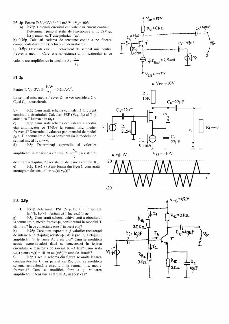
7/21/2019 Dispozitive si circuite electronice
http://slidepdf.com/reader/full/dispozitive-si-circuite-electronice-56d9365157aa2 44/45
P3. 2p Pentru T: VP=3V;β=0.1 mA/V2; VA=100V.
a) 0.75p Desenati circuitul echivalent în curent continuu.Determinati punctul static de functionare al T, Q(VDS,ID) şi aratati ca T este polarizat(a F).
h) 0.75p Calculati caderea de tensiune continua pe fiecarecomponenta din circuit (inclusiv condensatoare).i) 0.5p Desenati circuitul echivalent de semnal mic pentrufrecventa medii. Care este conexiunea amplificatoruluişi ce
valoare are amplificarea în tensiune Av=i
ovv
P1. 2p
Pentru T, VP=3V;β=2L
KW=0,2mA/V2.
La semnal mic, medie frecvenţă, se vor considera CG,CD şi CS – scurtcircuit.
b) 0,5p Cum arată schema echivalentă în curentcontinuu a circuitului? Calculaţi PSF (VDS, ID) al T şiar ătaţi că T lucrează în (a F).c) 0,5p Cum arată schema echivalentă a acestuietaj amplificator cu TMOS la semnal mic, mediefrecvenţă? Determinaţi valoarea parametrului de modelgm al T la semnal mic. Se va considera că în modelul desemnal mic al T, r o→∞. d) 0,5p Determinaţi expresiile şi valorile:
amplificării în tensiune a etajului, Av=i
o
vv
; rezistenţei
de intrare a etajului, R i; rezistenţei de ieşire a etajului, R o.e) 0,5p Dacă vi(t) are forma din figur ă, cum arată cronogramele tensiunilor: vo(t); vD(t)?
P.3. 2,5p
f) 0,75p Determinaţi PSF (VCE, IC) al T în ipotezaIB<<I1, IB<<I2. Ar ătaţi că T lucrează în a F.
g) 0,5p Cum arată schema echivalentă a circuituluila semnal mic, medie frecvenţă, considerând în modelul T
că r o→∞? În ce conexiune este T în acest etaj? h) 0,75p Care sunt expresiileşi valorile: rezistenţeide intrare R i a etajului; rezistenţei de ieşire R o a etajului;amplificării în tensiune Av a etajului? Cum se modifică aceste expresii/valori dacă se conectează la ieşireacircuitului o rezistenţă de sarcină R L=3 K Ω? Cum arată vo(t) pentru vi(t) = 10 sinωt [mV] în ambele situaţii? i) 0,5p Dacă în schema din figur ă se omite legareacondensatorului CE în paralel cu R E, cum se modifică schema echivalentă a circuitului la semnal mic, mediefrecvenţă? Cum se modifică formula şi valoareaamplificării în tensiune a etajului Av în acest caz?
VSS = -10V
~T
VDD =10V
vovi
IPol 0.8mA
CS 22μF
R L→
CD=22μF
R G 2,2M
CG=22 F
R D 15K
vD
20
-20
vi[mV]
t

7/21/2019 Dispozitive si circuite electronice
http://slidepdf.com/reader/full/dispozitive-si-circuite-electronice-56d9365157aa2 45/45
R B1 10K Ω
R B2 5K Ω
T
R C 2K Ω
R L 3Κ Ω
CB=47μF
CC 47μF
VCC=12VP.3. 2.5pPentru tranzistorul T, VBE , on=0,6V0.75p a) Cum arată schema echivalentă a circuitului încurent continuu? Care este PSF al T ?( )CE C V I ,0.75p b) Ce valori au parametrii de semnal mic aitranzistorului:β, r be, gm? Care este schema echivalenta pentru variatii a amplificatorului ? Se consider ă
.mA5,1=C I 0.5p c) In ce conexiune este amplificatorul ? Ce valoriau ?oiv R R A ,,0.5p d) Care sunt cronogramele semnalelor
pentru),(),(),( t it vt v C Oo ]mV[sin20)( t t vi ω = ? vi R E 1,7K Ω
vO
CΕ 47μF