Capitolul 1. Integrarea pe Scara Foarte Mare.
77
Capitolul 1. Integrarea pe Scara Foarte Mare. Integrarea pe Scara Foarte Mare a circuitelor electronice reprezinta una dintre tehnologiile de varf ale industriei moderne. Cunoscuta in engleza sub prescurtarea VLSI (Very Large Scale Integration) aceasta tehnologie asigura componentele de baza si structurile functionale necesare realizarii unei game extrem de largi de produse si sisteme, pentru cele mai diverse aplicatii, incepand cu cele de uz casnic si terminand cu cele pentru industria aerospatiala. Principalele avantaje ale produselor realizate in tehnologia ISFM se refera la implementarea unor sisteme cu o mare complexitate functionala in capsule de mici dimensiuni, in conditiile unui consum mic de putere si a unei fiabilitati extrem de ridicate. Fara utilizarea tehnologiei VLSI nu ar fi de conceput echipamnetele intalnite in bunurile de larg consum, intre care se pot mentiona: - masinile de spalat cu comanda programata, cuptoarele cu microunde, frigiderele; - echipamentele audio de mare fidelitate, televizoarele, aparatele de fotografiat, ceasurile electronice, sisteme de securitate pentru locuinte; - calculatoarele personale, calculatoarele personale ultramobile, IPod-urile calculatoarele de buzunar, jucariile electronice; - echipamentele medicale pentru masurarea tensiunii arteriale, echipamente portabile pentru masurarea si inregistrarea tensiunii, pulsului, electrocardiogramelor,echipamentele pentru asigurarea unei bune conditii fizice; - telefoanele mobile, pager-ele etc; - injectia electronica pentru automobile, calculatoare de bord, sensori pentru centurile de siguranta si pentru presiunea in anvelope, sisteme de alarmare etc. Incepand cu inventarea tranzistorului, in anul 1947, tehnologia dispozitivelor semiconductoare a evoluat continuu. Din punctul de vedere al complexitatii, circuitele integrate s-au dezvoltat exponential. Spre exemplu, primul microprocesor, pe 4 biti, aparut in anul 1971, avea circa 1700 de tranzistoare, iar in anul 1990 microprocesoarele pe 32 de biti aveau deja peste 150.000 de tranzistoare. Procesoarele moderne utilizeaza
Transcript of Capitolul 1. Integrarea pe Scara Foarte Mare.

Capitolul 1. Integrarea pe Scara Foarte Mare.
Integrarea pe Scara Foarte Mare a circuitelor electronice reprezinta una dintre
tehnologiile de varf ale industriei moderne. Cunoscuta in engleza sub prescurtarea VLSI
(Very Large Scale Integration) aceasta tehnologie asigura componentele de baza si
structurile functionale necesare realizarii unei game extrem de largi de produse si
sisteme, pentru cele mai diverse aplicatii, incepand cu cele de uz casnic si terminand cu
cele pentru industria aerospatiala.
Principalele avantaje ale produselor realizate in tehnologia ISFM se refera la
implementarea unor sisteme cu o mare complexitate functionala in capsule de mici
dimensiuni, in conditiile unui consum mic de putere si a unei fiabilitati extrem de
ridicate.
Fara utilizarea tehnologiei VLSI nu ar fi de conceput echipamnetele intalnite in bunurile
de larg consum, intre care se pot mentiona:
- masinile de spalat cu comanda programata, cuptoarele cu microunde,
frigiderele;
- echipamentele audio de mare fidelitate, televizoarele, aparatele de fotografiat,
ceasurile electronice, sisteme de securitate pentru locuinte;
- calculatoarele personale, calculatoarele personale ultramobile, IPod-urile
calculatoarele de buzunar, jucariile electronice;
- echipamentele medicale pentru masurarea tensiunii arteriale, echipamente
portabile pentru masurarea si inregistrarea tensiunii, pulsului,
electrocardiogramelor,echipamentele pentru asigurarea unei bune conditii fizice;
- telefoanele mobile, pager-ele etc;
- injectia electronica pentru automobile, calculatoare de bord, sensori pentru
centurile de siguranta si pentru presiunea in anvelope, sisteme de alarmare etc.
Incepand cu inventarea tranzistorului, in anul 1947, tehnologia dispozitivelor
semiconductoare a evoluat continuu. Din punctul de vedere al complexitatii, circuitele
integrate s-au dezvoltat exponential. Spre exemplu, primul microprocesor, pe 4 biti,
aparut in anul 1971, avea circa 1700 de tranzistoare, iar in anul 1990 microprocesoarele
pe 32 de biti aveau deja peste 150.000 de tranzistoare. Procesoarele moderne utilizeaza
peste zeci si sute de milioane de tranzistoare (Fig.1.). Toate aceste exemple demonstreaza
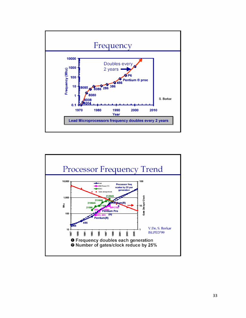
viabilitatea legii lui Moore, care apreciaza ca numarul de tranzistoare plasate pe o singura
pastila se dubleaza la circa 18 luni.
Fig. 1. Evolutia in timp a numarului de tranzistoare pe pastila pentru cateva
procesoare Intel
Perfectionarea proceselor tehnologice in domneiul circuitelor integrate a permis, de
asemenea, reducerea dimensiunilor dispozitivelor, ceea ce se poate exemplifica prin
reducerea lungimii canalului tranzistorului elementar de la 5 μm, in 1985, la 0,35 μm, in
1997 si la 0,70 nm in 2005. In acelasi timp au crescut dimensiunile discurilor din siliciul
monocristalin, care reprezinta suportul pe care se realizeaza structurile larg integrate.
Evolutia in timp a unor elemente definitorii pentru circuitele integrate se poate urmari in
tabelul de mai jos.
Intarzierea in propagarea semnalelor s-a redus cu trei ordine de marime in ultimii 20 de
ani, ceea ce se reflecta in cresterea frecventei ceasului microprocesoarelor de la circa
1MHz in 1975 la pesete 1 GHz in anul 2000. In acelasi timp s-au redus in mod continuu
costurile de fabricatie. Astfel, in cazul memoriilor RAM, costul pe bit s-a micsorat de la
circa 1 cent, in 1970, la 10-4
-10-5
centi, in prezent.
Actualmente, pentru circuitele integrate folosite in calculatoarele electronice, se folosesc
numeroase tehnologii, care se pot grupa in tehnologii bipolare si tehnologii MOS
Tehnologii bipolare:
• TTL (Transistor Transistor Logic):
- TTL-S (Schottky TTL),
- TTL-LS (Low-Power Schottky TTL)
- TTL-AS (Advanced Schottky TTL),
- TTL-ALS (Advanced Low-power Schottky TTL),
- FAST (Fairchild Advanced Schottky TTL).
• ECL (Emitter Coupled Logic).
• I2L (Integrated Injection Logic).
Tehnologii MOS:
• PMOS (MOS canal P).
• NMOS (MOS canal N):
- HMOS (High performance MOS).
• CMOS (Complementary MOS):
- HCMOS (High density CMOS),
- ACL (Advanced CMOS Logic).
• MNOS (Metal Nitride Oxide Semiconductor):
- FAMOS (Floating gate Avalanche injection MOS),
- FLOTOX (FLOating gate Tunnel Oxide).
4
Circuitele integrate care se folosesc in constructia calculatoarelor se plaseaza in categoriile:
standard, specifice aplicatiilor (ASIC - Application Specific Integrated Circuits) si
programabile/configurabile.
La randul lor circuitele ASIC se impart in:
• Circuite personalizate la cerere ( Semi-Custom ):
- Circuite predifuzate ( Gate Arrays ).
• Circuite realizate la comanda ( Custom ):
- Circuite precaracterizate ( Standard Cells ),
- Circuite realizate complet la cerere ( Full Custom ).
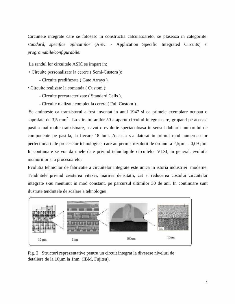
Se aminteste ca tranzistorul a fost inventat in anul 1947 si ca primele exemplare ocupau o
suprafata de 3,5 mm2 . La sfirsitul anilor 50 a aparut circuitul integrat care, grupand pe aceeasi
pastila mai multe tranzistoare, a avut o evolutie spectaculoasa in sensul dublarii numarului de
componente pe pastila, la fiecare 18 luni. Aceasta s-a datorat in primul rand numeroaselor
perfectionari ale proceselor tehnologice, care au permis rezolutii de ordinul a 2,5µm – 0,09 µm.
In continuare se vor da unele date privind tehnologiile circuitelor VLSI, in general, evolutia
memoriilor si a procesoarelor
Evolutia tehnicilor de fabricatie a circuitelor integrate este unica in istoria industriei moderne.
Tendintele privind cresterea vitezei, marirea densitatii, cat si reducerea costului circuitelor
integrate s-au mentinut in mod constant, pe parcursul ultimilor 30 de ani. In continuare sunt
ilustrate tendintele de scalare a tehnologiei.
Fig. 2. Structuri reprezentative pentru un circuit integrat la diverese niveluri de
detaliere de la 10µm la 1nm. (IBM, Fujitsu).
5
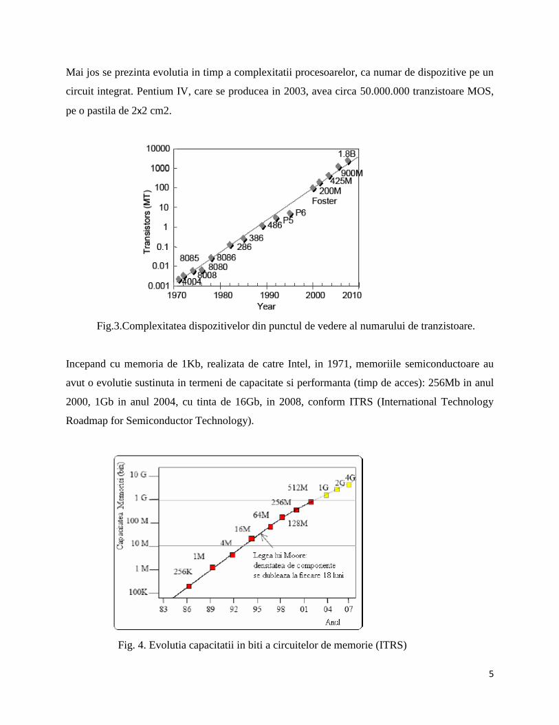
Mai jos se prezinta evolutia in timp a complexitatii procesoarelor, ca numar de dispozitive pe un
circuit integrat. Pentium IV, care se producea in 2003, avea circa 50.000.000 tranzistoare MOS,
pe o pastila de 2x2 cm2.
Fig.3.Complexitatea dispozitivelor din punctul de vedere al numarului de tranzistoare.
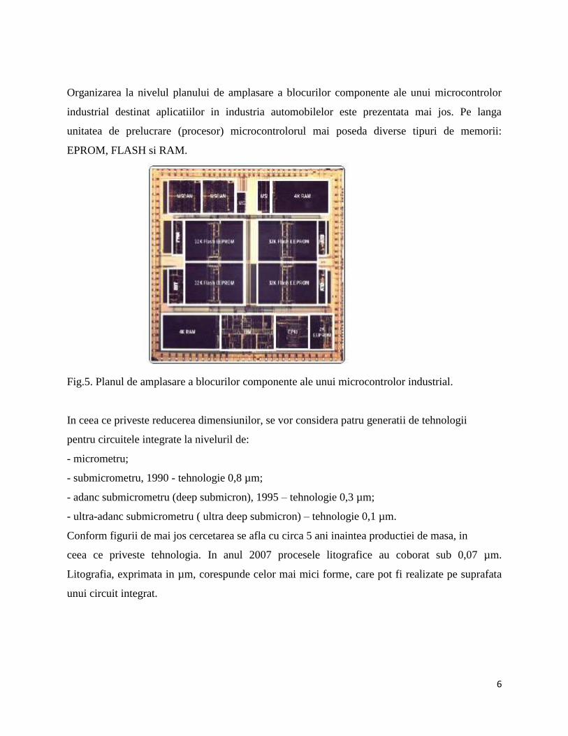
Incepand cu memoria de 1Kb, realizata de catre Intel, in 1971, memoriile semiconductoare au
avut o evolutie sustinuta in termeni de capacitate si performanta (timp de acces): 256Mb in anul
2000, 1Gb in anul 2004, cu tinta de 16Gb, in 2008, conform ITRS (International Technology
Roadmap for Semiconductor Technology).
Fig. 4. Evolutia capacitatii in biti a circuitelor de memorie (ITRS)
6
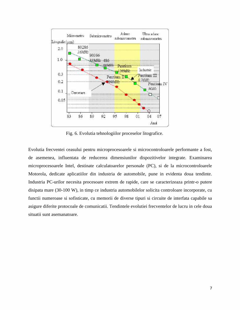
Organizarea la nivelul planului de amplasare a blocurilor componente ale unui microcontrolor
industrial destinat aplicatiilor in industria automobilelor este prezentata mai jos. Pe langa
unitatea de prelucrare (procesor) microcontrolorul mai poseda diverse tipuri de memorii:
EPROM, FLASH si RAM.
Fig.5. Planul de amplasare a blocurilor componente ale unui microcontrolor industrial.
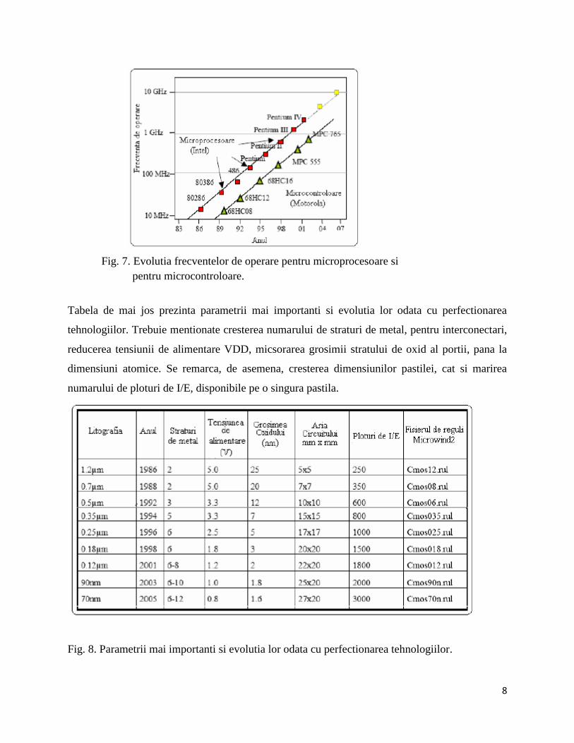
In ceea ce priveste reducerea dimensiunilor, se vor considera patru generatii de tehnologii
pentru circuitele integrate la niveluril de:
- micrometru;
- submicrometru, 1990 - tehnologie 0,8 µm;
- adanc submicrometru (deep submicron), 1995 – tehnologie 0,3 µm;
- ultra-adanc submicrometru ( ultra deep submicron) – tehnologie 0,1 µm.
Conform figurii de mai jos cercetarea se afla cu circa 5 ani inaintea productiei de masa, in
ceea ce priveste tehnologia. In anul 2007 procesele litografice au coborat sub 0,07 µm.
Litografia, exprimata in µm, corespunde celor mai mici forme, care pot fi realizate pe suprafata
unui circuit integrat.
7
Fig. 6. Evolutia tehnologiilor proceselor litografice.
Evolutia frecventei ceasului pentru microprocesoarele si microcontroloarele performante a fost,
de asemenea, influentata de reducerea dimensiunilor dispozitivelor integrate. Examinarea
microprocesoarele Intel, destinate calculatoarelor personale (PC), si de la microcontroloarele
Motorola, dedicate aplicatiilor din industria de automobile, pune in evidenta doua tendinte.
Industria PC-urilor necesita procesoare extrem de rapide, care se caracterizeaza printr-o putere
disipata mare (30-100 W), in timp ce industria automobilelor solicita controloare incorporate, cu
functii numeroase si sofisticate, cu memorii de diverse tipuri si circuite de interfata capabile sa
asigure diferite protocoale de comunicatii. Tendintele evolutiei frecventelor de lucru in cele doua
situatii sunt asemanatoare.
8
Fig. 7. Evolutia frecventelor de operare pentru microprocesoare si
pentru microcontroloare.
Tabela de mai jos prezinta parametrii mai importanti si evolutia lor odata cu perfectionarea
tehnologiilor. Trebuie mentionate cresterea numarului de straturi de metal, pentru interconectari,
reducerea tensiunii de alimentare VDD, micsorarea grosimii stratului de oxid al portii, pana la
dimensiuni atomice. Se remarca, de asemena, cresterea dimensiunilor pastilei, cat si marirea
numarului de ploturi de I/E, disponibile pe o singura pastila.
Fig. 8. Parametrii mai importanti si evolutia lor odata cu perfectionarea tehnologiilor.
9
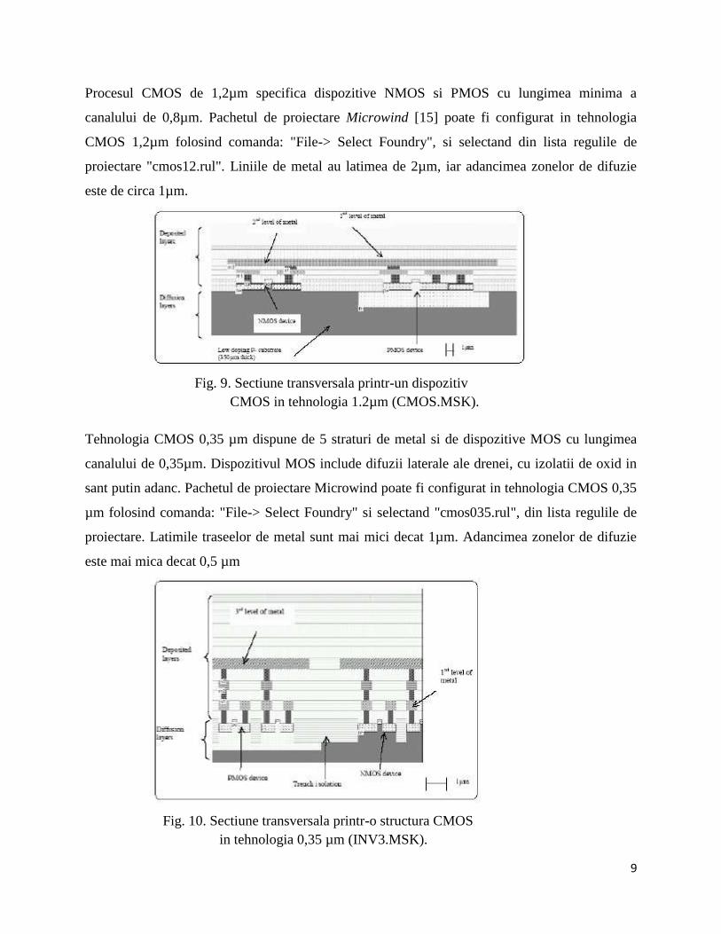
Procesul CMOS de 1,2µm specifica dispozitive NMOS si PMOS cu lungimea minima a
canalului de 0,8µm. Pachetul de proiectare Microwind [15] poate fi configurat in tehnologia
CMOS 1,2µm folosind comanda: "File-> Select Foundry", si selectand din lista regulile de
proiectare "cmos12.rul". Liniile de metal au latimea de 2µm, iar adancimea zonelor de difuzie
este de circa 1µm.
Fig. 9. Sectiune transversala printr-un dispozitiv
CMOS in tehnologia 1.2µm (CMOS.MSK).
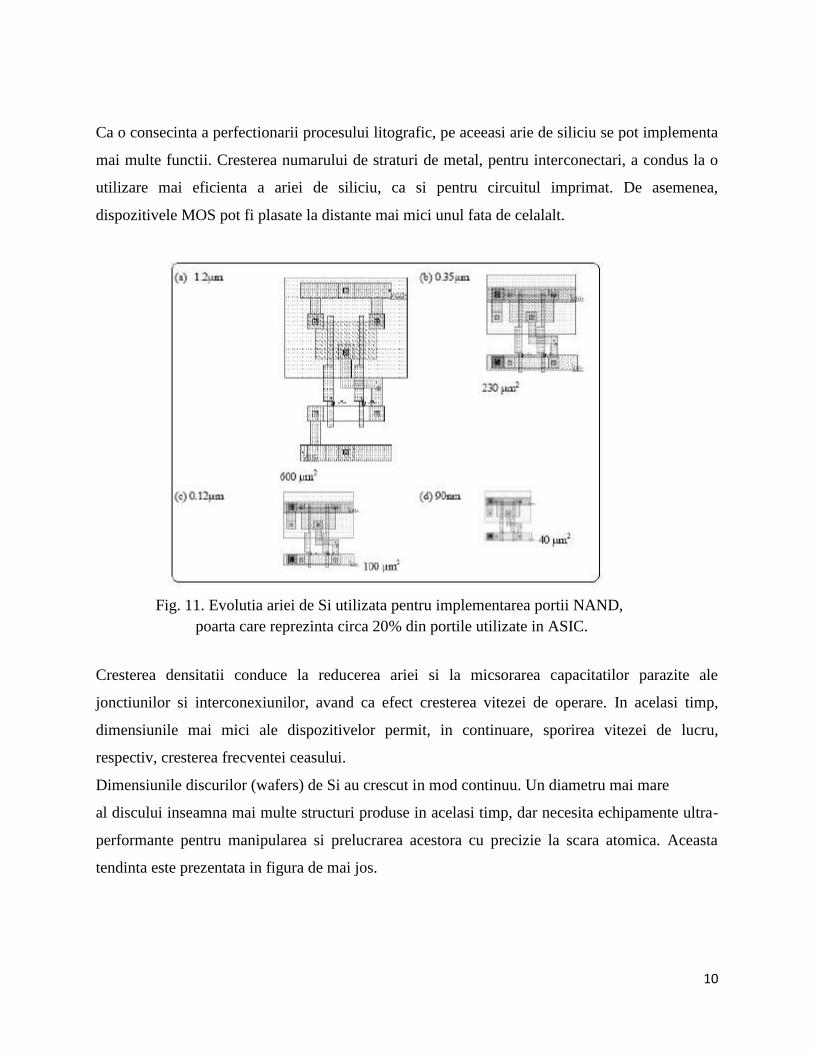
Tehnologia CMOS 0,35 µm dispune de 5 straturi de metal si de dispozitive MOS cu lungimea
canalului de 0,35µm. Dispozitivul MOS include difuzii laterale ale drenei, cu izolatii de oxid in
sant putin adanc. Pachetul de proiectare Microwind poate fi configurat in tehnologia CMOS 0,35
µm folosind comanda: "File-> Select Foundry" si selectand "cmos035.rul", din lista regulile de
proiectare. Latimile traseelor de metal sunt mai mici decat 1µm. Adancimea zonelor de difuzie
este mai mica decat 0,5 µm
Fig. 10. Sectiune transversala printr-o structura CMOS
in tehnologia 0,35 µm (INV3.MSK).
10
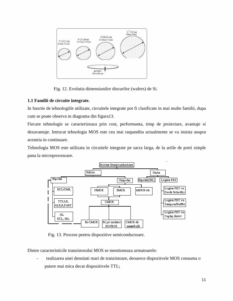
Ca o consecinta a perfectionarii procesului litografic, pe aceeasi arie de siliciu se pot implementa
mai multe functii. Cresterea numarului de straturi de metal, pentru interconectari, a condus la o
utilizare mai eficienta a ariei de siliciu, ca si pentru circuitul imprimat. De asemenea,
dispozitivele MOS pot fi plasate la distante mai mici unul fata de celalalt.
Fig. 11. Evolutia ariei de Si utilizata pentru implementarea portii NAND,
poarta care reprezinta circa 20% din portile utilizate in ASIC.
Cresterea densitatii conduce la reducerea ariei si la micsorarea capacitatilor parazite ale
jonctiunilor si interconexiunilor, avand ca efect cresterea vitezei de operare. In acelasi timp,
dimensiunile mai mici ale dispozitivelor permit, in continuare, sporirea vitezei de lucru,
respectiv, cresterea frecventei ceasului.
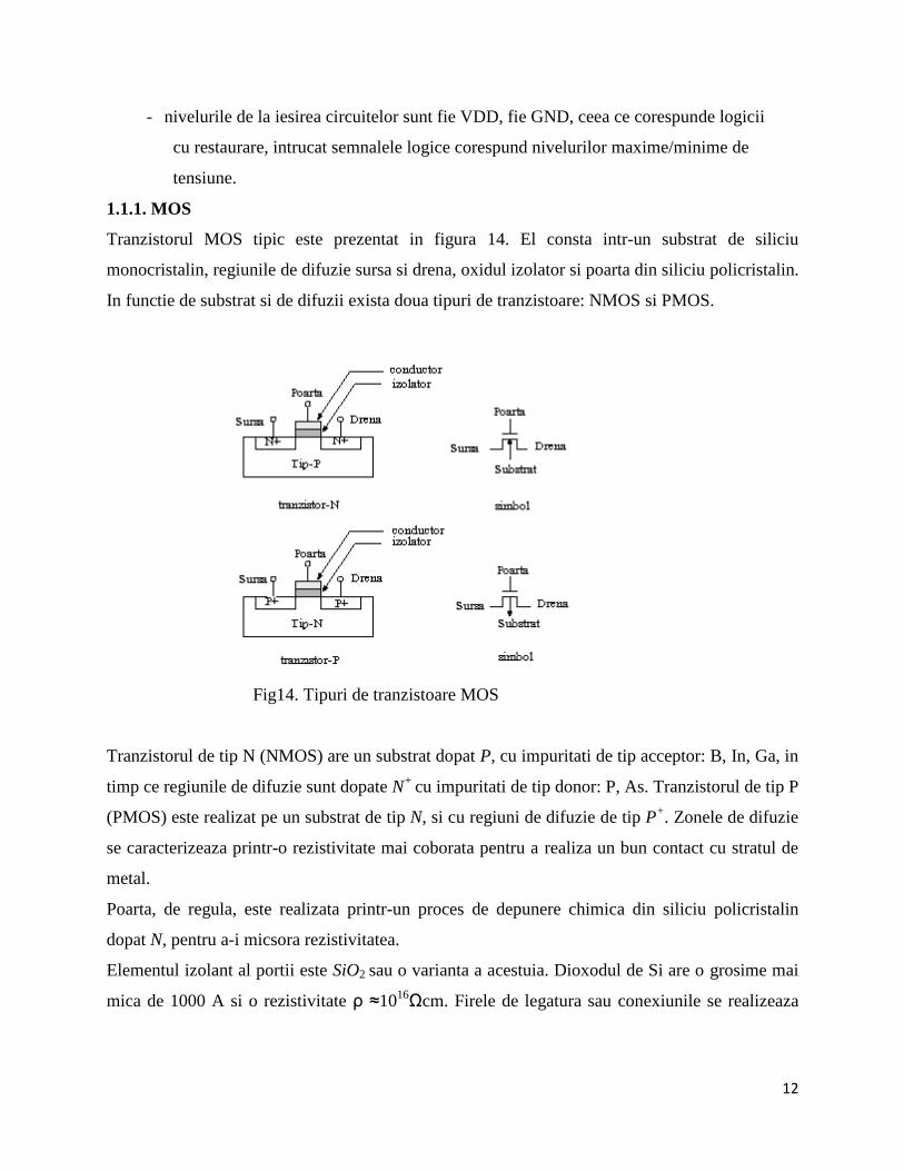
Dimensiunile discurilor (wafers) de Si au crescut in mod continuu. Un diametru mai mare
al discului inseamna mai multe structuri produse in acelasi timp, dar necesita echipamente ultra-
performante pentru manipularea si prelucrarea acestora cu precizie la scara atomica. Aceasta
tendinta este prezentata in figura de mai jos.
11
Fig. 12. Evolutia dimensiunilor discurilor (wafers) de Si.
1.1 Familii de circuite integrate.
In functie de tehnologiile utilizate, circuitele integrate pot fi clasificate in mai multe familii, dupa
cum se poate observa in diagrama din figura13.
Fiecare tehnologie se caracterizeaza prin cost, performanta, timp de proiectare, avantaje si
dezavantaje. Intrucat tehnologia MOS este cea mai raspandita actualmente se va insista asupra
acesteia in continuare.
Tehnologia MOS este utilizata in circuitele integrate pe sacra larga, de la ariile de porti simple
pana la microprocesoare.
Fig. 13. Procese pentru dispozitive semiconductoare.
Dintre caracteristicile tranzistorului MOS se mentioneaza urmatoarele:
- realizarea unei densitati mari de tranzistoare, deoarece dispozitvele MOS consuma o
putere mai mica decat dispozitivele TTL;
12
- nivelurile de la iesirea circuitelor sunt fie VDD, fie GND, ceea ce corespunde logicii
cu restaurare, intrucat semnalele logice corespund nivelurilor maxime/minime de
tensiune.
1.1.1. MOS
Tranzistorul MOS tipic este prezentat in figura 14. El consta intr-un substrat de siliciu
monocristalin, regiunile de difuzie sursa si drena, oxidul izolator si poarta din siliciu policristalin.
In functie de substrat si de difuzii exista doua tipuri de tranzistoare: NMOS si PMOS.
Fig14. Tipuri de tranzistoare MOS
Tranzistorul de tip N (NMOS) are un substrat dopat P, cu impuritati de tip acceptor: B, In, Ga, in
timp ce regiunile de difuzie sunt dopate N+
cu impuritati de tip donor: P, As. Tranzistorul de tip P
(PMOS) este realizat pe un substrat de tip N, si cu regiuni de difuzie de tip P+. Zonele de difuzie
se caracterizeaza printr-o rezistivitate mai coborata pentru a realiza un bun contact cu stratul de
metal.
Poarta, de regula, este realizata printr-un proces de depunere chimica din siliciu policristalin
dopat N, pentru a-i micsora rezistivitatea.
Elementul izolant al portii este SiO2 sau o varianta a acestuia. Dioxodul de Si are o grosime mai
mica de 1000 A si o rezistivitate ρ ≈1016Ωcm. Firele de legatura sau conexiunile se realizeaza
13
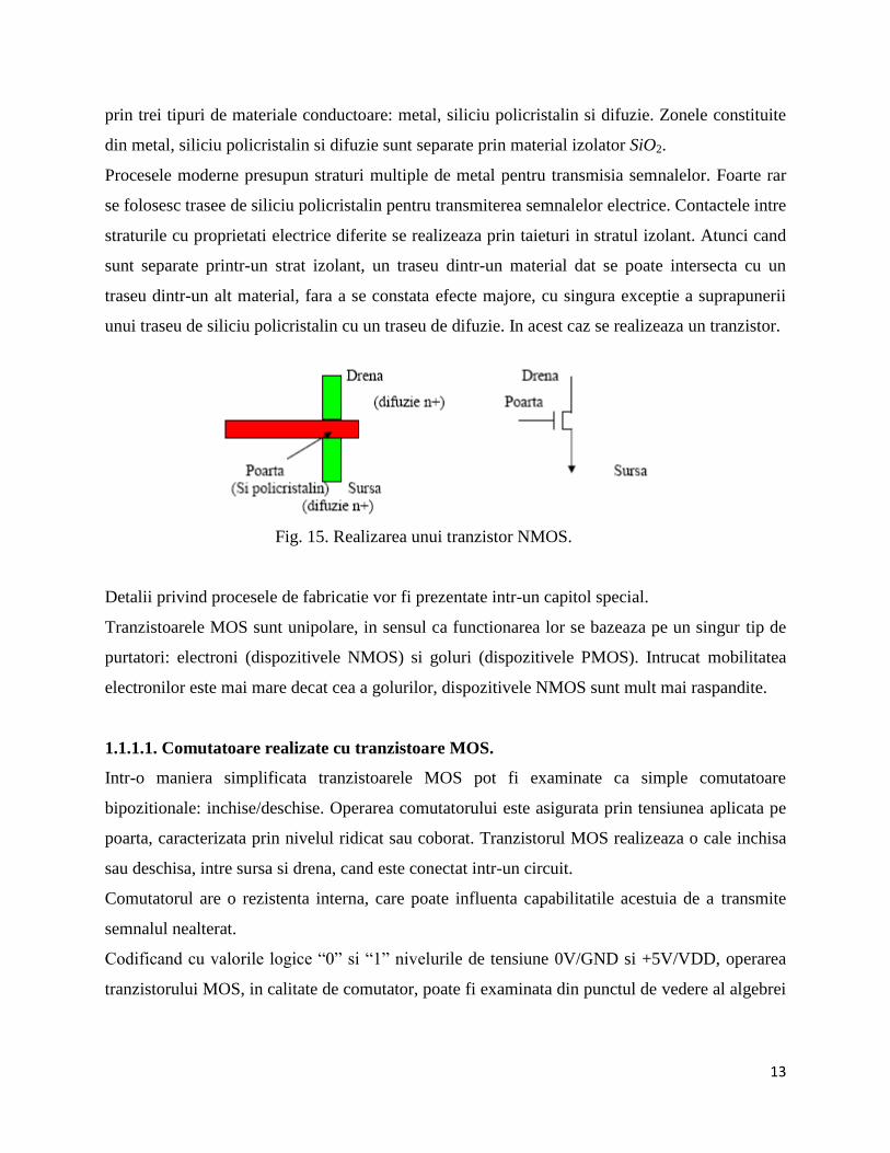
prin trei tipuri de materiale conductoare: metal, siliciu policristalin si difuzie. Zonele constituite
din metal, siliciu policristalin si difuzie sunt separate prin material izolator SiO2.
Procesele moderne presupun straturi multiple de metal pentru transmisia semnalelor. Foarte rar
se folosesc trasee de siliciu policristalin pentru transmiterea semnalelor electrice. Contactele intre
straturile cu proprietati electrice diferite se realizeaza prin taieturi in stratul izolant. Atunci cand
sunt separate printr-un strat izolant, un traseu dintr-un material dat se poate intersecta cu un
traseu dintr-un alt material, fara a se constata efecte majore, cu singura exceptie a suprapunerii
unui traseu de siliciu policristalin cu un traseu de difuzie. In acest caz se realizeaza un tranzistor.
Fig. 15. Realizarea unui tranzistor NMOS.
Detalii privind procesele de fabricatie vor fi prezentate intr-un capitol special.
Tranzistoarele MOS sunt unipolare, in sensul ca functionarea lor se bazeaza pe un singur tip de
purtatori: electroni (dispozitivele NMOS) si goluri (dispozitivele PMOS). Intrucat mobilitatea
electronilor este mai mare decat cea a golurilor, dispozitivele NMOS sunt mult mai raspandite.
1.1.1.1. Comutatoare realizate cu tranzistoare MOS.
Intr-o maniera simplificata tranzistoarele MOS pot fi examinate ca simple comutatoare
bipozitionale: inchise/deschise. Operarea comutatorului este asigurata prin tensiunea aplicata pe
poarta, caracterizata prin nivelul ridicat sau coborat. Tranzistorul MOS realizeaza o cale inchisa
sau deschisa, intre sursa si drena, cand este conectat intr-un circuit.
Comutatorul are o rezistenta interna, care poate influenta capabilitatile acestuia de a transmite
semnalul nealterat.
Codificand cu valorile logice “0” si “1” nivelurile de tensiune 0V/GND si +5V/VDD, operarea
tranzistorului MOS, in calitate de comutator, poate fi examinata din punctul de vedere al algebrei
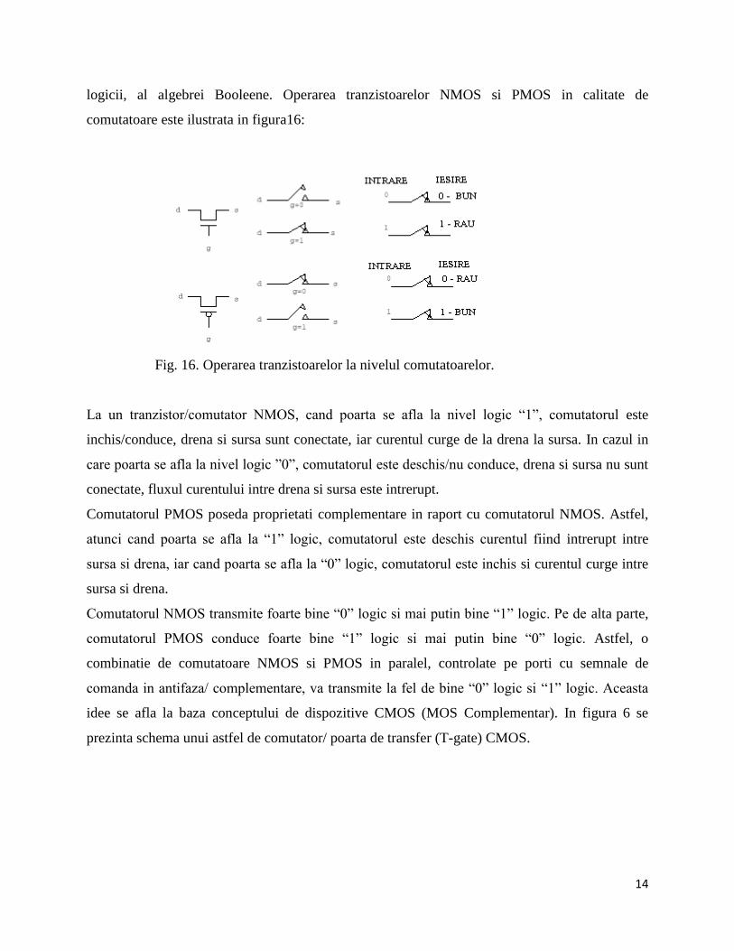
14
logicii, al algebrei Booleene. Operarea tranzistoarelor NMOS si PMOS in calitate de
comutatoare este ilustrata in figura16:
Fig. 16. Operarea tranzistoarelor la nivelul comutatoarelor.
La un tranzistor/comutator NMOS, cand poarta se afla la nivel logic “1”, comutatorul este
inchis/conduce, drena si sursa sunt conectate, iar curentul curge de la drena la sursa. In cazul in
care poarta se afla la nivel logic ”0”, comutatorul este deschis/nu conduce, drena si sursa nu sunt
conectate, fluxul curentului intre drena si sursa este intrerupt.
Comutatorul PMOS poseda proprietati complementare in raport cu comutatorul NMOS. Astfel,
atunci cand poarta se afla la “1” logic, comutatorul este deschis curentul fiind intrerupt intre
sursa si drena, iar cand poarta se afla la “0” logic, comutatorul este inchis si curentul curge intre
sursa si drena.
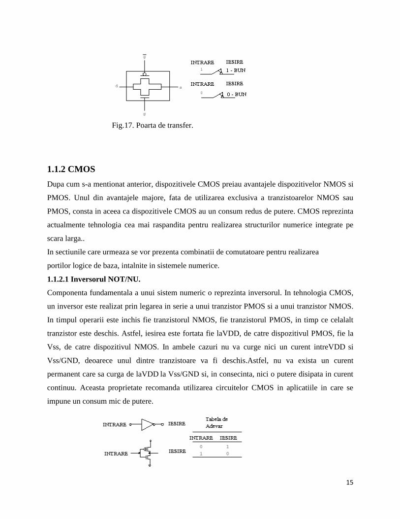
Comutatorul NMOS transmite foarte bine “0” logic si mai putin bine “1” logic. Pe de alta parte,
comutatorul PMOS conduce foarte bine “1” logic si mai putin bine “0” logic. Astfel, o
combinatie de comutatoare NMOS si PMOS in paralel, controlate pe porti cu semnale de
comanda in antifaza/ complementare, va transmite la fel de bine “0” logic si “1” logic. Aceasta
idee se afla la baza conceptului de dispozitive CMOS (MOS Complementar). In figura 6 se
prezinta schema unui astfel de comutator/ poarta de transfer (T-gate) CMOS.
15
Fig.17. Poarta de transfer.
1.1.2 CMOS
Dupa cum s-a mentionat anterior, dispozitivele CMOS preiau avantajele dispozitivelor NMOS si
PMOS. Unul din avantajele majore, fata de utilizarea exclusiva a tranzistoarelor NMOS sau
PMOS, consta in aceea ca dispozitivele CMOS au un consum redus de putere. CMOS reprezinta
actualmente tehnologia cea mai raspandita pentru realizarea structurilor numerice integrate pe
scara larga..
In sectiunile care urmeaza se vor prezenta combinatii de comutatoare pentru realizarea
portilor logice de baza, intalnite in sistemele numerice.
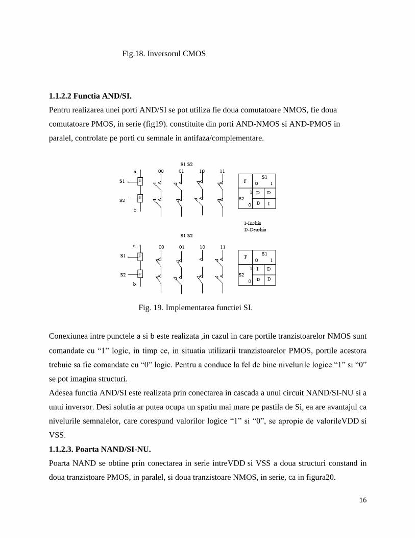
1.1.2.1 Inversorul NOT/NU.
Componenta fundamentala a unui sistem numeric o reprezinta inversorul. In tehnologia CMOS,
un inversor este realizat prin legarea in serie a unui tranzistor PMOS si a unui tranzistor NMOS.
In timpul operarii este inchis fie tranzistorul NMOS, fie tranzistorul PMOS, in timp ce celalalt
tranzistor este deschis. Astfel, iesirea este fortata fie laVDD, de catre dispozitivul PMOS, fie la
Vss, de catre dispozitivul NMOS. In ambele cazuri nu va curge nici un curent intreVDD si
Vss/GND, deoarece unul dintre tranzistoare va fi deschis.Astfel, nu va exista un curent
permanent care sa curga de laVDD la Vss/GND si, in consecinta, nici o putere disipata in curent
continuu. Aceasta proprietate recomanda utilizarea circuitelor CMOS in aplicatiile in care se
impune un consum mic de putere.
16
Fig.18. Inversorul CMOS
1.1.2.2 Functia AND/SI.
Pentru realizarea unei porti AND/SI se pot utiliza fie doua comutatoare NMOS, fie doua
comutatoare PMOS, in serie (fig19). constituite din porti AND-NMOS si AND-PMOS in
paralel, controlate pe porti cu semnale in antifaza/complementare.
Fig. 19. Implementarea functiei SI.
Conexiunea intre punctele a si b este realizata ,in cazul in care portile tranzistoarelor NMOS sunt
comandate cu “1” logic, in timp ce, in situatia utilizarii tranzistoarelor PMOS, portile acestora
trebuie sa fie comandate cu “0” logic. Pentru a conduce la fel de bine nivelurile logice “1” si “0”
se pot imagina structuri.
Adesea functia AND/SI este realizata prin conectarea in cascada a unui circuit NAND/SI-NU si a
unui inversor. Desi solutia ar putea ocupa un spatiu mai mare pe pastila de Si, ea are avantajul ca
nivelurile semnalelor, care corespund valorilor logice “1” si “0”, se apropie de valorileVDD si
VSS.
1.1.2.3. Poarta NAND/SI-NU.
Poarta NAND se obtine prin conectarea in serie intreVDD si VSS a doua structuri constand in
doua tranzistoare PMOS, in paralel, si doua tranzistoare NMOS, in serie, ca in figura20.
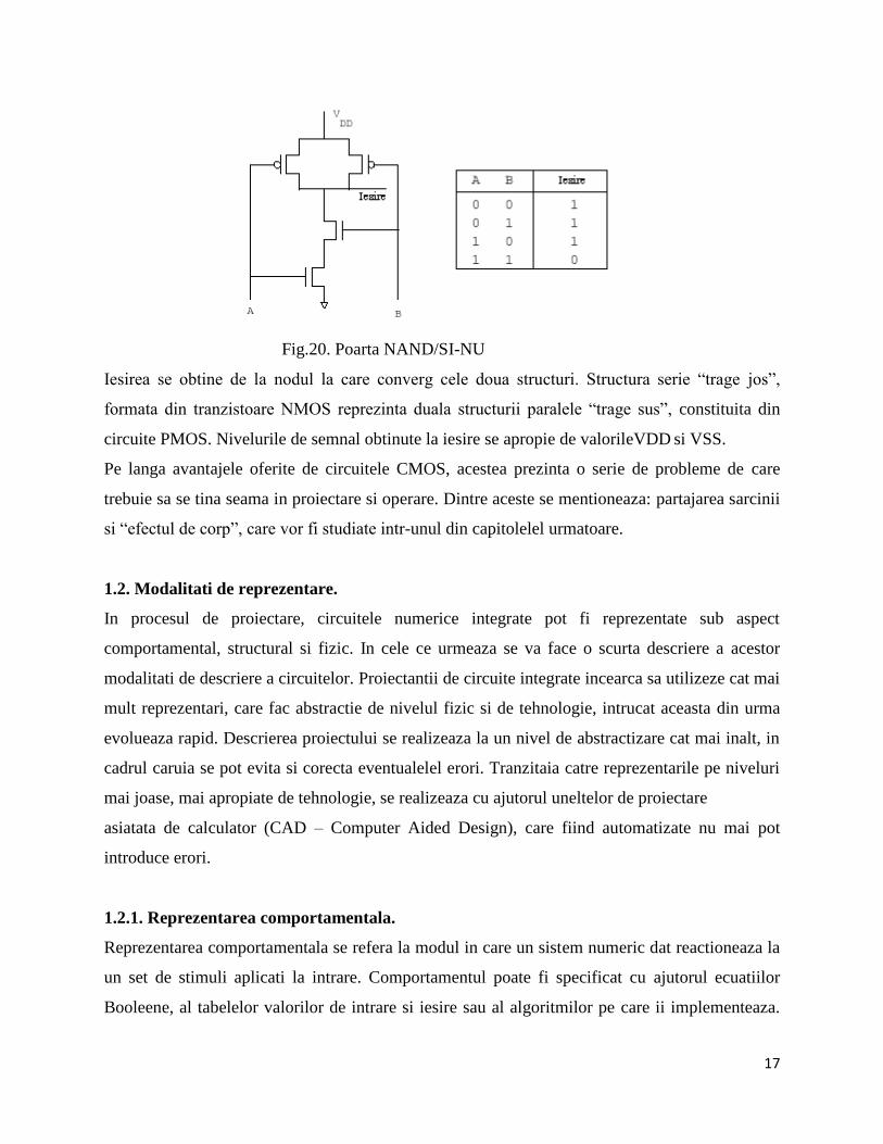
17
Fig.20. Poarta NAND/SI-NU
Iesirea se obtine de la nodul la care converg cele doua structuri. Structura serie “trage jos”,
formata din tranzistoare NMOS reprezinta duala structurii paralele “trage sus”, constituita din
circuite PMOS. Nivelurile de semnal obtinute la iesire se apropie de valorileVDD si VSS.
Pe langa avantajele oferite de circuitele CMOS, acestea prezinta o serie de probleme de care
trebuie sa se tina seama in proiectare si operare. Dintre aceste se mentioneaza: partajarea sarcinii
si “efectul de corp”, care vor fi studiate intr-unul din capitolelel urmatoare.
1.2. Modalitati de reprezentare.
In procesul de proiectare, circuitele numerice integrate pot fi reprezentate sub aspect
comportamental, structural si fizic. In cele ce urmeaza se va face o scurta descriere a acestor
modalitati de descriere a circuitelor. Proiectantii de circuite integrate incearca sa utilizeze cat mai
mult reprezentari, care fac abstractie de nivelul fizic si de tehnologie, intrucat aceasta din urma
evolueaza rapid. Descrierea proiectului se realizeaza la un nivel de abstractizare cat mai inalt, in
cadrul caruia se pot evita si corecta eventualelel erori. Tranzitaia catre reprezentarile pe niveluri
mai joase, mai apropiate de tehnologie, se realizeaza cu ajutorul uneltelor de proiectare
asiatata de calculator (CAD – Computer Aided Design), care fiind automatizate nu mai pot
introduce erori.
1.2.1. Reprezentarea comportamentala.
Reprezentarea comportamentala se refera la modul in care un sistem numeric dat reactioneaza la
un set de stimuli aplicati la intrare. Comportamentul poate fi specificat cu ajutorul ecuatiilor
Booleene, al tabelelor valorilor de intrare si iesire sau al algoritmilor pe care ii implementeaza.
18
Acestia din urma pot fi descrisi in limbaje de programare de nivel inalt sau in limbaje
specializate pentru descrierea hardware-lui: VHDL (Very High Speed Integrated Circuit
Hardware Description Language), Verilog, ELLA etc.
Scopul urmarit de catre diversele sisteme moderne de proiectare consta in transformarea
specificatiilor de operare a sistemului, date la nivelul cel mai inalt posibil de descriere, intr-un
proiect viabil, in timpul cel mai scurt.
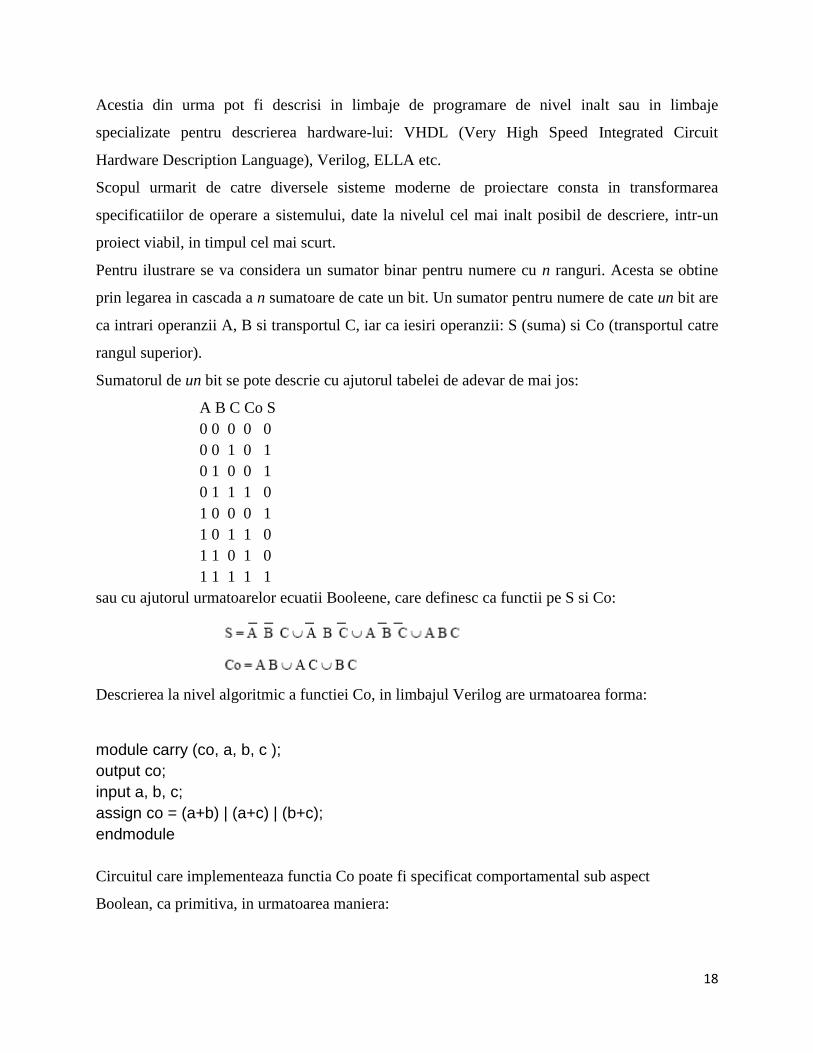
Pentru ilustrare se va considera un sumator binar pentru numere cu n ranguri. Acesta se obtine
prin legarea in cascada a n sumatoare de cate un bit. Un sumator pentru numere de cate un bit are
ca intrari operanzii A, B si transportul C, iar ca iesiri operanzii: S (suma) si Co (transportul catre
rangul superior).
Sumatorul de un bit se pote descrie cu ajutorul tabelei de adevar de mai jos:
A B C Co S
0 0 0 0 0
0 0 1 0 1
0 1 0 0 1
0 1 1 1 0
1 0 0 0 1
1 0 1 1 0
1 1 0 1 0
1 1 1 1 1
sau cu ajutorul urmatoarelor ecuatii Booleene, care definesc ca functii pe S si Co:
Descrierea la nivel algoritmic a functiei Co, in limbajul Verilog are urmatoarea forma:
module carry (co, a, b, c );
output co;
input a, b, c;
assign co = (a+b) | (a+c) | (b+c);
endmodule
Circuitul care implementeaza functia Co poate fi specificat comportamental sub aspect
Boolean, ca primitiva, in urmatoarea maniera:
19
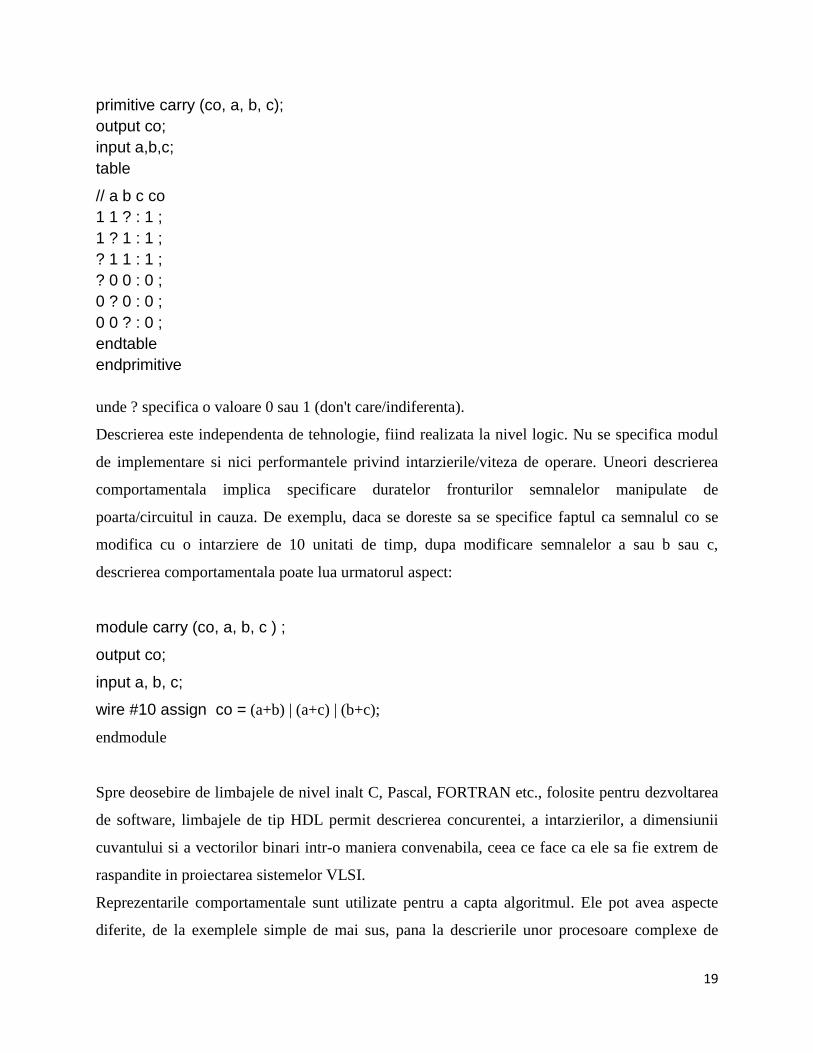
primitive carry (co, a, b, c);
output co;
input a,b,c;
table
// a b c co
1 1 ? : 1 ;
1 ? 1 : 1 ;
? 1 1 : 1 ;
? 0 0 : 0 ;
0 ? 0 : 0 ;
0 0 ? : 0 ;
endtable
endprimitive
unde ? specifica o valoare 0 sau 1 (don't care/indiferenta).
Descrierea este independenta de tehnologie, fiind realizata la nivel logic. Nu se specifica modul
de implementare si nici performantele privind intarzierile/viteza de operare. Uneori descrierea
comportamentala implica specificare duratelor fronturilor semnalelor manipulate de
poarta/circuitul in cauza. De exemplu, daca se doreste sa se specifice faptul ca semnalul co se
modifica cu o intarziere de 10 unitati de timp, dupa modificare semnalelor a sau b sau c,
descrierea comportamentala poate lua urmatorul aspect:
module carry (co, a, b, c ) ;
output co;
input a, b, c;
wire #10 assign co = (a+b) | (a+c) | (b+c);
endmodule
Spre deosebire de limbajele de nivel inalt C, Pascal, FORTRAN etc., folosite pentru dezvoltarea
de software, limbajele de tip HDL permit descrierea concurentei, a intarzierilor, a dimensiunii
cuvantului si a vectorilor binari intr-o maniera convenabila, ceea ce face ca ele sa fie extrem de
raspandite in proiectarea sistemelor VLSI.
Reprezentarile comportamentale sunt utilizate pentru a capta algoritmul. Ele pot avea aspecte
diferite, de la exemplele simple de mai sus, pana la descrierile unor procesoare complexe de
20
semnal. Avantajul lor consta in aceea ca permit descrierea si verificarea proiectului la nivel
functional. Dezavantajul major se refera la faptul ca descrierea comportamentala nu se poate
implementa direct si eficient in hardware.
1.2.2. Reprezentarea structurala.
Reprezentarea structurala a unui sistem numeric prezinta modul in care sunt interconectate
componentele sistemului in vederea realizarii unei functii date sau a unui anumit comportament.
Descrierea structurala consta intr-o lista de module si de interconexiuni ale acestora.
Nivelurile abstracte ierarhice, ale descrierii structurale se refera la: module, porti, comutatoare si
circuite. Pe masura parcurgerii ierarhiei de niveluri se evidentiaza detalii privind implementarea.
Pentru exemplificare se va considera cazul unui sumator pe 4 biti, constituit prin conectarea in
cascada a patru sumatoare de cate un bit. Descrierea este realizata in Verilog HDL.
module add4 (s,c4,ci,a,b) ;
input [3:0]a,b;
input ci;
output [3:0]s;
output c4;
wire [2:0]co;
add a0 (co[0],s[0],a[0],b[0],ci);
add a1 (co[1],s[1],a[1],b[1],c[0]);
add a2 (co[2],s[2],a[2],b[2],c[1]);
add a3 (c4,s[3],a[3],b[3],co[2]);
endmodule
Dupa declararea modulului add4, in urmatoarele patru linii sunt definite intrarile si iesirile, iar in
linia a cincea se specifica vectorul binar intern, pe trei biti, co. In continuare se apeleaza de patru
ori modulul add, a carui descriere se da mai jos:
module add (co,s,a,b,c) ;
input a,b,c;
output s,co;
sum s1(s,a,b,c);
carry c1(co,a,b,c);
endmodule
21
Modulul de mai sus specifica un sumator de un bit, care este constituit, la randul sau,
din doua module pentru calculul sumei (sum) si al transportului (carry).
module carry (co,a,b,c) ;
input a,b,c;
output co;
wire x,y,z;
and g1 (x,a,b);
and g2 (y,a,c);
and g3 (z,b,c);
or g4 (co,x,y,z);
endmodule
Descrierea de mai sus este independenta de tehnologie deoarece au fost utilizate porti generice,
fara a se specifica implementarea lor.
In cazul unei implementari in tehnologie CMOS, modulul carry poate fi descris la nivelul
tranzistoarelor componente.
Tranzistoarele sunt descrise prin: tip, nume si conexiunile drenei, sursei si portii:
Tip-tranzistor|Nume|Drena(Iesire)|Sursa(Data)|Poarta(comanda)
nmos n1 i1 vss a
Descrierea modulului carry, implementat in tehnologie CMOS,
are urmatorul aspect:
module carry (co,a,b,c) ;
input a,b,c;
output co;
wire i1,i2,i3,i4,cn;
nmos n1 (i1,vss,a);
nmos n2 (i1,vss,b);
nmos n3 (cn,i1,c);
nmos n4 (i2,vss,b);
nmos n5 (cn,i2,a);
pmos p1 (i3,vdd,b);
pmos p2 (cn,i3,a);
pmos p3 (cn,i4,c);
pmos p4 (i4,vdd,b);
22
pmos p5 (i4,vdd,a);
pmos p6 (co,vdd,cn);
nmos n6 (co,vss,cn);
endmodule
In comparatie cu descrierea comportamentala, descrierea structurala contine detalii referitoare la
nodurile interne, la conexiunile intre componentele primitive sau elementele de comutatie
folosite pentru implementare. La nivelurile superioare de descriere ale modulului aceste
conexiuni nu sunt relevante.
Descrierile de mai sus nu furnizeaza informatii referitoere la comportarea temporala a modulului
carry, deoarece ele sunt realizate la nivelul portilor, la nivelul circuitelor de comutatie.
Unul din limbajele de descriere structurala care surprinde, printre altele, si comportarea
temporala a modulelor este limbajul SPICE.
In SPICE tranzistoarele sunt specificate prin inregistrari, care contin urmatoarele campuri:
Mnume drena poarta sursa substrat tip W = latime L = lungime AD = aria drenei
AS = aria sursei
Numele tranzistoarelor incep cu majuscula M. Tipul specifica daca este un tranzistor
nmos sau pmos.
Capacitatile sunt descrise astfel:
Cnume nodul-1 nodul-2 valoare
De exemplu un NAND cu doua intrari poate fi descris in SPICE dupa cum urmeaza:
.SUBCKT NANDVDD VSS A B OUT
MN1 I1 A VSS VSS NFET
MN2 OUT B I1 VSS NFET
MP1 OUT A VDD VDD PFET
MP2 OUT B VDD VDD PFET
.ENDS
unde A si B reprezinta terminalele de intrare, iar OUT este terminalul de iesire.
Reprezentarea structurala permite introducerea unor parametrii suplimentari si a
dimensiunulor tranzistoarelor.
Astfel, specificarea unei porti NAND are aspectul de mai jos:
23
.SUBCKT NAND VDD VSS A B OUT
MN1 I1 A VSS VSS NFET W=8U L=4U AD=64P AS=64P
MN2 OUT B I1 VSS NFET W=8U L=4U AD=64P AS=64P
MP1 OUT A VDD VDD PFET W=16U L=4U AD=128P AS=128P
MP2 OUT B VDD VDD PFET W=16U L=4U AS=128P AS=128P
CA A VSS 50fF
CB B VSS 50fF
COUT OUT VSS 100fF
.ENDS
Simulatorul SPICE calculeaza capacitatile parazite interne ale tranzistoarelor MOS, folosind
modele adecvate, pe baza dimensiunilor specificate pentru dispozitive.
Pentru a introduce si influenta capacitatilor traseelor interne, prin care se conecteaza
dispozitivele, se evalueaza valorile acestor capacitati ce se conecteaza la nodurile
corespunzatoare. Astfel, modulul poate fi caracterizat sub aspectul vitezei de operare, al puterii
disipate si al conectivitatii. Rezultatele obtinute in urma simularii: intarzieri, duratele fronturilor
crescatoare si cazatoare etc, pot fi furnizate descrierilor la nivel logic sub forma de intarzieri.
1.2.3. Reprezentarea fizica.
Descrierea fizica a sistemelor numerice furnizeaza informatii privind modul de constructie al
unui circuit particular, care va avea o structura si o comportare date.
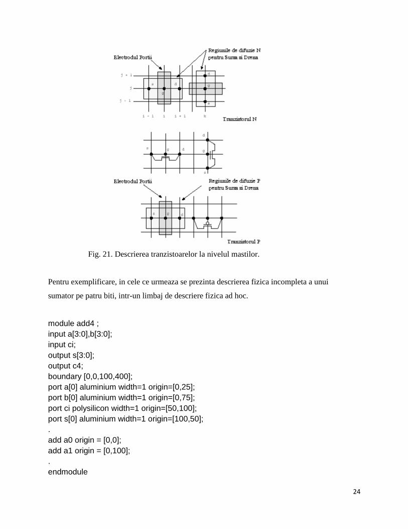
Intr-un proces de realizare a circuitelor integrate, specificarea fizica cu nivelul cel mai coborat o
reprezinta descriera geometrica a mastilor fotografice, pentru fiecare etapa a procesului
tehnologic. Un exemplu de descriere geometrica este dat, la nivelul mastilor pentru tranzistoare
NMOS si PMOS, in figura 21.
Descrierea fizica comporta, de asemenea, mai multe niveluri de abstractie. La nivel de modul,
planul fizic pentru un sumator cu patru biti poate fi definit ca un dreptunghi sau un poligon, care
specifica limitele externe pentru toata geometria sumatorului, un set de chemari de submodule si
o colectie de porturi. Fiecare port corespunde unei conexiuni de I/E in descrierea structurala a
sumatorului. Pentru fiecare port se specifica pozitia, stratul, numele, si latimea.
24
Fig. 21. Descrierea tranzistoarelor la nivelul mastilor.
Pentru exemplificare, in cele ce urmeaza se prezinta descrierea fizica incompleta a unui
sumator pe patru biti, intr-un limbaj de descriere fizica ad hoc.
module add4 ;
input a[3:0],b[3:0];
input ci;
output s[3:0];
output c4;
boundary [0,0,100,400];
port a[0] aluminium width=1 origin=[0,25];
port b[0] aluminium width=1 origin=[0,75];
port ci polysilicon width=1 origin=[50,100];
port s[0] aluminium width=1 origin=[100,50];
.
add a0 origin = [0,0];
add a1 origin = [0,100];
.
endmodule
25
Porturile sunt indicate prin cuvantul cheie port, iar chemarile submodulelor ce reprezinta
sumatoare pe un bit sunt specificate prin cuvintul cheie add.
La cel mai jos nivel de descriere fizica se fac chemari la tranzistoare, fire si la conexiuni.
Acestea specifica dimensiunile dreptunghiurilor, care se implementeaza pe diverse straturi ale
procesului CMOS. Aici nu se va intra in aceste detalii, poarta CMOS fiind tratata ca un
dreptunghi cu frontiere date si cu porturile necesare. Fiecare port are o pozitie, un strat de
conectare, o latime si un nume. Aceste informatii pot fi utilizate de catre un program automat de
trasare, care va asigura interconectarea acestor module cu alte proiecte.
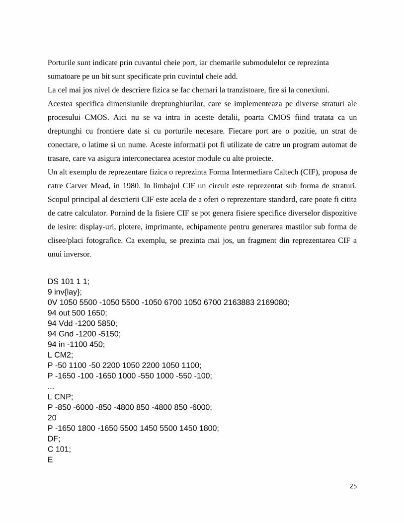
Un alt exemplu de reprezentare fizica o reprezinta Forma Intermediara Caltech (CIF), propusa de
catre Carver Mead, in 1980. In limbajul CIF un circuit este reprezentat sub forma de straturi.
Scopul principal al descrierii CIF este acela de a oferi o reprezentare standard, care poate fi citita
de catre calculator. Pornind de la fisiere CIF se pot genera fisiere specifice diverselor dispozitive
de iesire: display-uri, plotere, imprimante, echipamente pentru generarea mastilor sub forma de
clisee/placi fotografice. Ca exemplu, se prezinta mai jos, un fragment din reprezentarea CIF a
unui inversor.
DS 101 1 1;
9 inv{lay};
0V 1050 5500 -1050 5500 -1050 6700 1050 6700 2163883 2169080;
94 out 500 1650;
94 Vdd -1200 5850;
94 Gnd -1200 -5150;
94 in -1100 450;
L CM2;
P -50 1100 -50 2200 1050 2200 1050 1100;
P -1650 -100 -1650 1000 -550 1000 -550 -100;
...
L CNP;
P -850 -6000 -850 -4800 850 -4800 850 -6000;
20
P -1650 1800 -1650 5500 1450 5500 1450 1800;
DF;
C 101;
E
26
Se intelege de la sine ca un proiectant nu va fi interesat sa desfasoare activitatea de proiectare la
acest nivel de reprezentare/abstractizare. El va prefera descrierile la nivel inalt ale sistemelor ce
urmeaza a fi implementate. Aceste descrieri, dupa simulari si verificari exhaustive, vor fi
compilate in fisiere de tip CIF, in vederea obtinerii mastilor si a unor simulari mai detaliate,
avand in vedere atat aspectele geometrice, cat si cele privitoare la procesele tehnologice utilizate.
1.3. Etapele proiectarii.
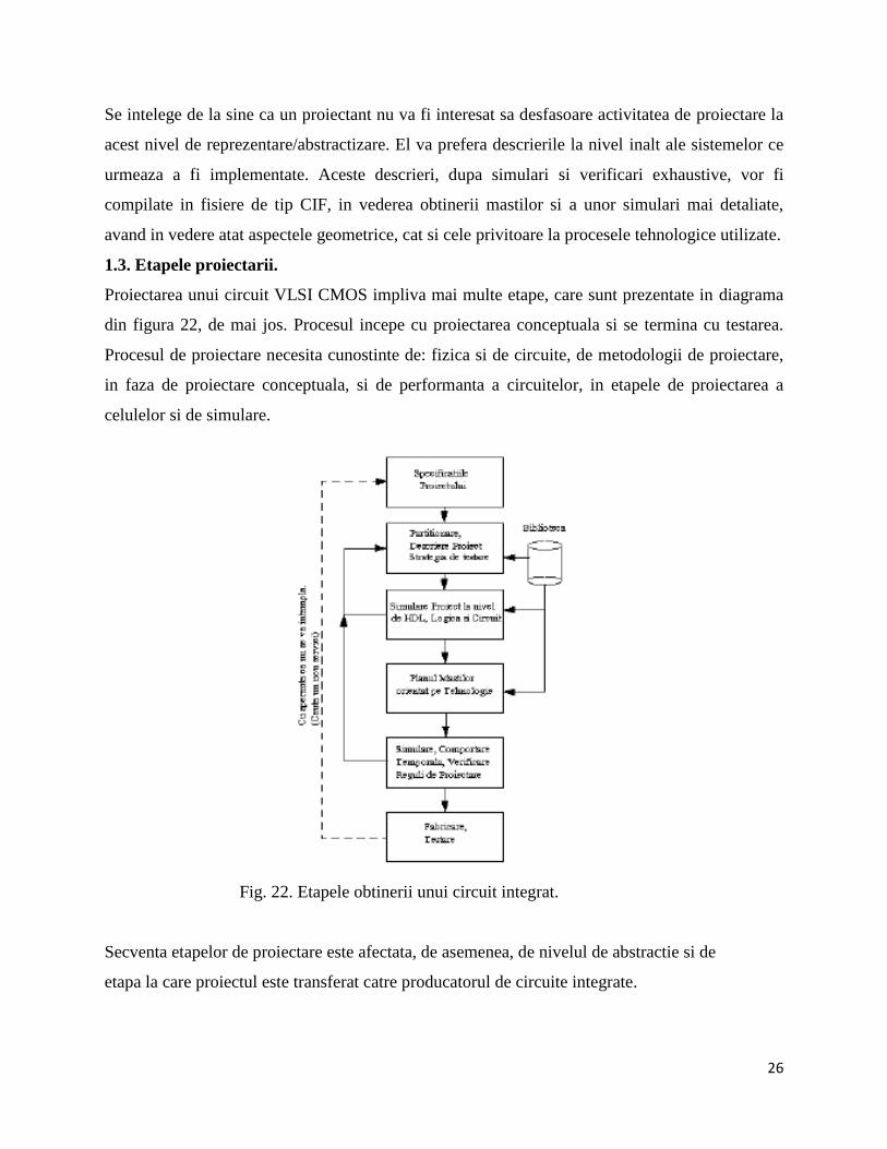
Proiectarea unui circuit VLSI CMOS impliva mai multe etape, care sunt prezentate in diagrama
din figura 22, de mai jos. Procesul incepe cu proiectarea conceptuala si se termina cu testarea.
Procesul de proiectare necesita cunostinte de: fizica si de circuite, de metodologii de proiectare,
in faza de proiectare conceptuala, si de performanta a circuitelor, in etapele de proiectarea a
celulelor si de simulare.
Fig. 22. Etapele obtinerii unui circuit integrat.
Secventa etapelor de proiectare este afectata, de asemenea, de nivelul de abstractie si de
etapa la care proiectul este transferat catre producatorul de circuite integrate.
27
Captarea specificarii proiectului reprezinta una dintre cele mai dificile sarcini. De cele mai multe
ori proiectul este specificat in limbaj natural, ceea ce poate induce un anumit grad de imprecizie,
fara a mai mentiona imposibilitatea executiei acestei descrieri, in sensul simularii
comportamentale. O specificare executabila permite simularea si verificarea functionalitatii.
Secventa de proiectare implica utilizarea unei biblioteci, care va contine modele functionale
descrise la nivel inalt, modele de simulare corecte, cat si modelele unor circuite integrate reale.
Standardizarea si utilizarea bibliotecilor, permit reutilizarea unor proiecte sau a unor parti de
proiect, cat si reducerea timpului de proiectare.
Secventa de proiectare include numeroase bucle de reactie. De exemplu, dupa proiectare
schemelor logice ale circuitelor se efectueaza simulari. Daca simularea pune in evidenta o eroare
logica, proiectantul va reveni la schemele logice si va corecta eroare, dupa care va efectua din
nou simularea. Secventa de proiectare descrisa mai sus poate sa capete aspecte usor diferite, in
cadrul unor companii diferite.
28
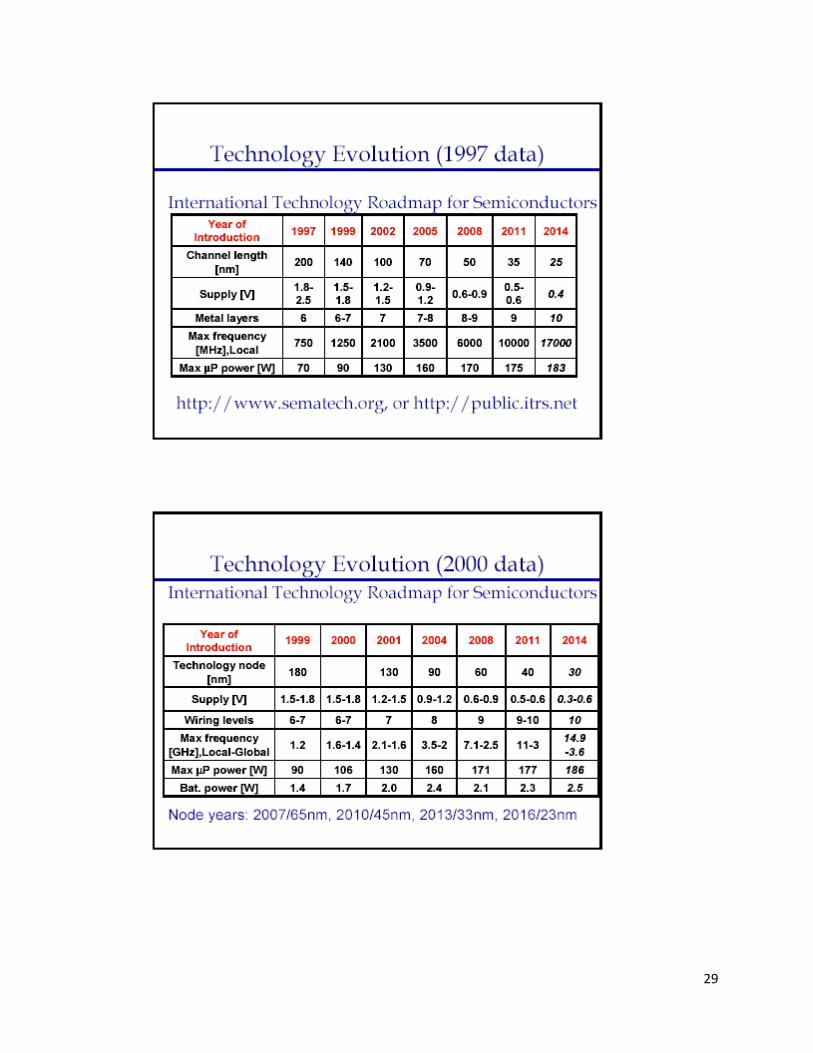
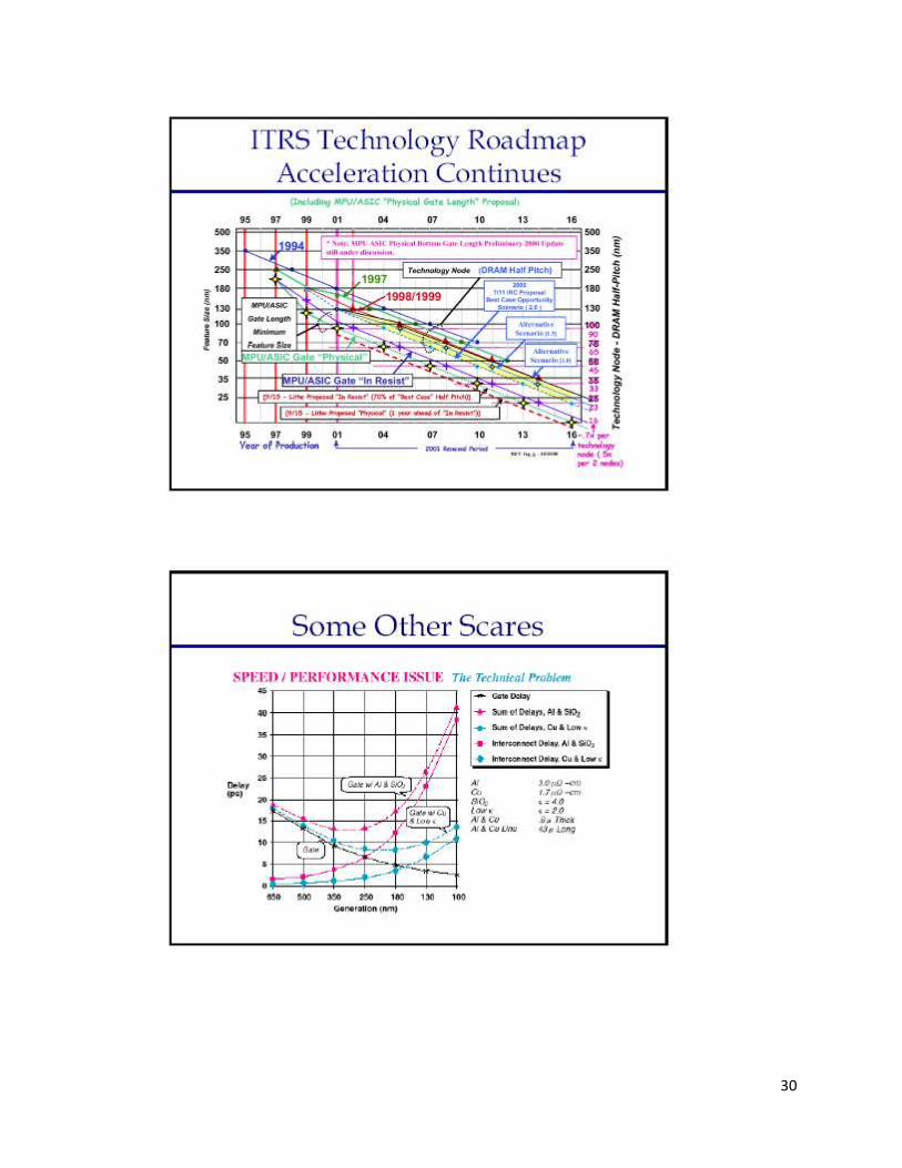
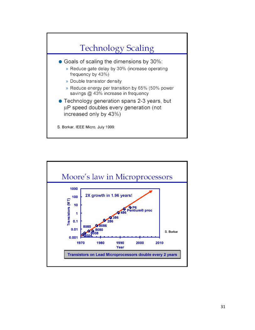
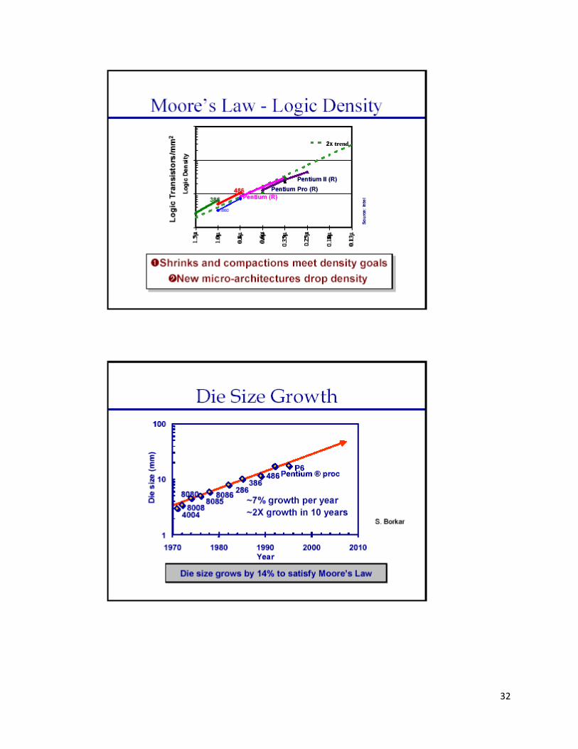
Anexa 1. International Technology Roadmap for Semiconductors.
29
30
31
32
33
34
35
36
37
38
39
40
41
42
43
44
45
46
47
48
ANEXA. 2 Exemple de procesoare modern Intel.
Marking of modern Intel processors
Just to warm up - a few words on the marking of Intel's modern
processors. I presume, the pinout of the new processors is clear - it is
the well-known and familiar LGA775. All the more or less modern Intel CPU models - both high-end and mainstream - have long migrated to
LGA775.
But the marking of CPUs has undergone serious changes and now is
made up of 5 elements - a combination of the letter prefix followed by
a 4-digit numerical index. It makes sense decoding the 5-digit marking
49
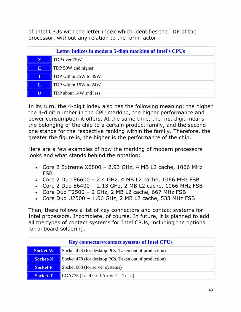
of Intel CPUs with the letter index which identifies the TDP of the
processor, without any relation to the form factor.
Letter indices in modern 5-digit marking of Intel's CPUs
X TDP over 75W
E TDP 50W and higher
T TDP within 25W to 49W
L TDP within 15W to 24W
U TDP about 14W and less
In its turn, the 4-digit index also has the following meaning: the higher the 4-digit number in the CPU marking, the higher performance and
power consumption it offers. At the same time, the first digit means the belonging of the chip to a certain product family, and the second
one stands for the respective ranking within the family. Therefore, the
greater the figure is, the higher is the performance of the chip.
Here are a few examples of how the marking of modern processors
looks and what stands behind the notation:
Core 2 Extreme X6800 – 2.93 GHz, 4 MB L2 cache, 1066 MHz
FSB Core 2 Duo E6600 – 2.4 GHz, 4 MB L2 cache, 1066 MHz FSB
Core 2 Duo E6400 – 2.13 GHz, 2 MB L2 cache, 1066 MHz FSB
Core Duo T2500 – 2 GHz, 2 MB L2 cache, 667 MHz FSB Core Duo U2500 – 1.06 GHz, 2 MB L2 cache, 533 MHz FSB
Then, there follows a list of key connectors and contact systems for Intel processors. Incomplete, of course. In future, it is planned to add
all the types of contact systems for Intel CPUs, including the options
for onboard soldering.
Key connectors/contact systems of Intel CPUs
Socket-W Socket 423 (for desktop PCs. Taken out of production)
Socket-N Socket 478 (for desktop PCs. Taken out of production)
Socket-F Socket 603 (for server systems)
Socket-T LGA775 (Land Grid Array. T - Tejas)
50
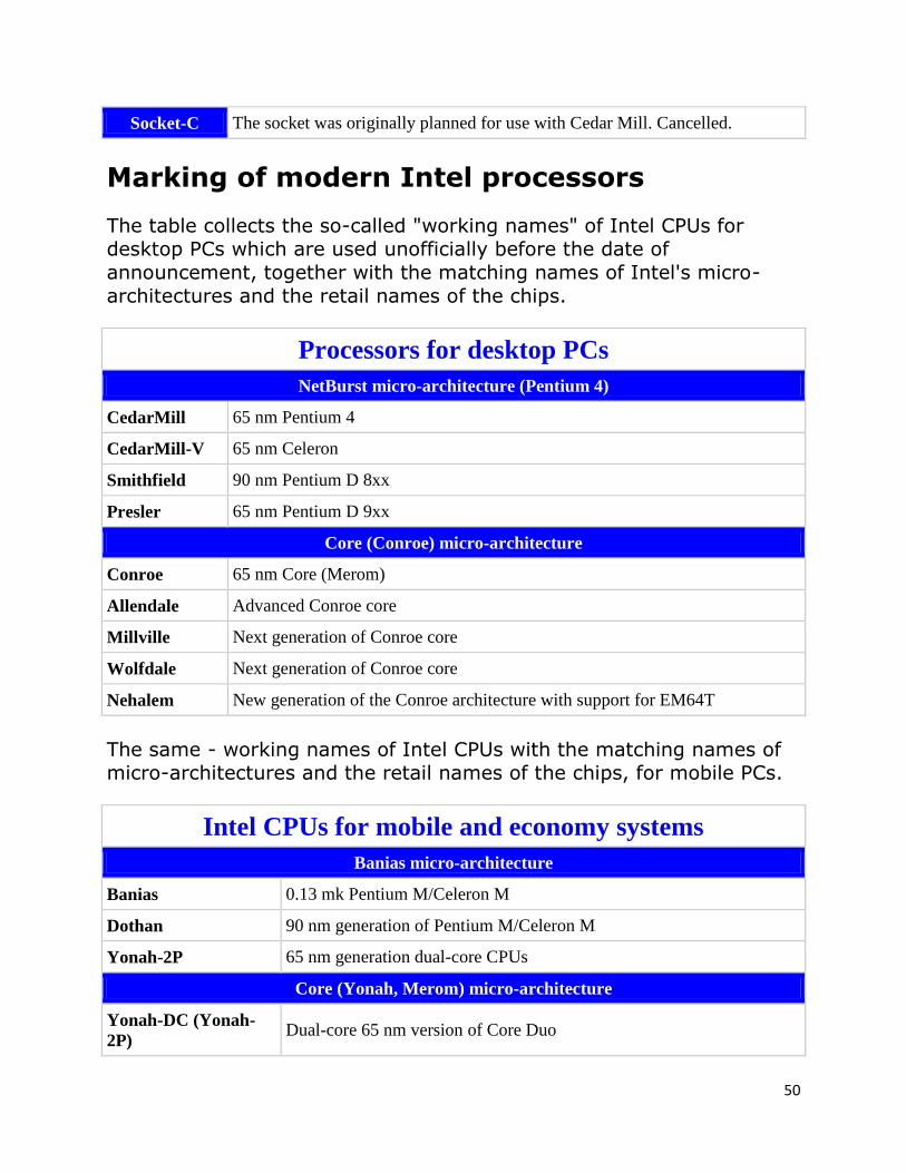
Socket-C The socket was originally planned for use with Cedar Mill. Cancelled.
Marking of modern Intel processors
The table collects the so-called "working names" of Intel CPUs for desktop PCs which are used unofficially before the date of
announcement, together with the matching names of Intel's micro-
architectures and the retail names of the chips.
Processors for desktop PCs
NetBurst micro-architecture (Pentium 4)
CedarMill 65 nm Pentium 4
CedarMill-V 65 nm Celeron
Smithfield 90 nm Pentium D 8xx
Presler 65 nm Pentium D 9xx
Core (Conroe) micro-architecture
Conroe 65 nm Core (Merom)
Allendale Advanced Conroe core
Millville Next generation of Conroe core
Wolfdale Next generation of Conroe core
Nehalem New generation of the Conroe architecture with support for EM64T
The same - working names of Intel CPUs with the matching names of micro-architectures and the retail names of the chips, for mobile PCs.
Intel CPUs for mobile and economy systems
Banias micro-architecture
Banias 0.13 mk Pentium M/Celeron M
Dothan 90 nm generation of Pentium M/Celeron M
Yonah-2P 65 nm generation dual-core CPUs
Core (Yonah, Merom) micro-architecture
Yonah-DC (Yonah-
2P) Dual-core 65 nm version of Core Duo
51
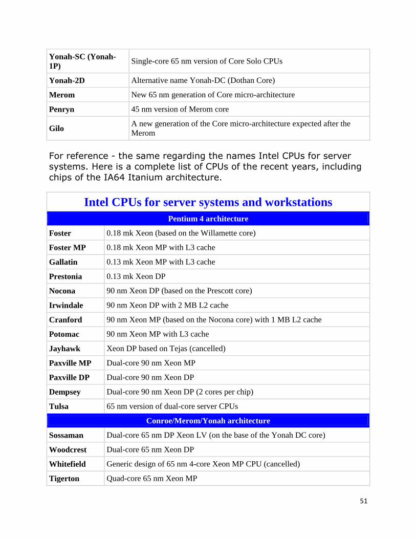
Yonah-SC (Yonah-
1P) Single-core 65 nm version of Core Solo CPUs
Yonah-2D Alternative name Yonah-DC (Dothan Core)
Merom New 65 nm generation of Core micro-architecture
Penryn 45 nm version of Merom core
Gilo A new generation of the Core micro-architecture expected after the
Merom
For reference - the same regarding the names Intel CPUs for server systems. Here is a complete list of CPUs of the recent years, including
chips of the IA64 Itanium architecture.
Intel CPUs for server systems and workstations
Pentium 4 architecture
Foster 0.18 mk Xeon (based on the Willamette core)
Foster MP 0.18 mk Xeon MP with L3 cache
Gallatin 0.13 mk Xeon MP with L3 cache
Prestonia 0.13 mk Xeon DP
Nocona 90 nm Xeon DP (based on the Prescott core)
Irwindale 90 nm Xeon DP with 2 MB L2 cache
Cranford 90 nm Xeon MP (based on the Nocona core) with 1 MB L2 cache
Potomac 90 nm Xeon MP with L3 cache
Jayhawk Xeon DP based on Tejas (cancelled)
Paxville MP Dual-core 90 nm Xeon MP
Paxville DP Dual-core 90 nm Xeon DP
Dempsey Dual-core 90 nm Xeon DP (2 cores per chip)
Tulsa 65 nm version of dual-core server CPUs
Conroe/Merom/Yonah architecture
Sossaman Dual-core 65 nm DP Xeon LV (on the base of the Yonah DC core)
Woodcrest Dual-core 65 nm Xeon DP
Whitefield Generic design of 65 nm 4-core Xeon MP CPU (cancelled)
Tigerton Quad-core 65 nm Xeon MP
52
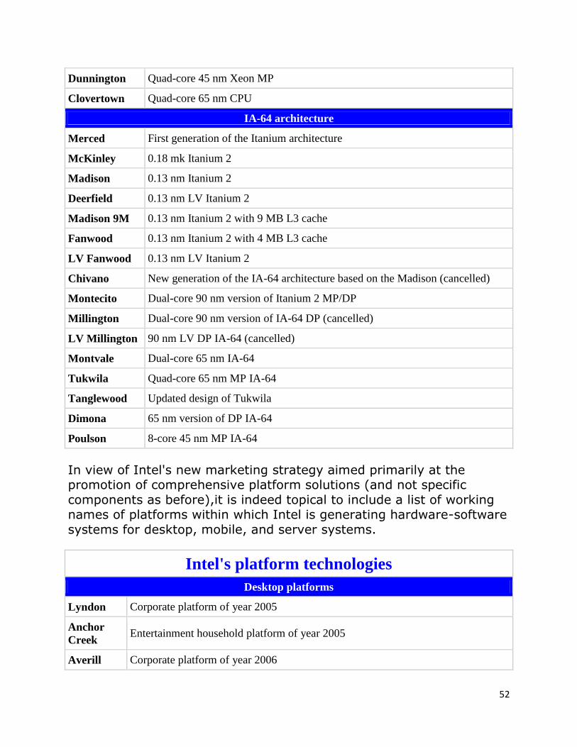
Dunnington Quad-core 45 nm Xeon MP
Clovertown Quad-core 65 nm CPU
IA-64 architecture
Merced First generation of the Itanium architecture
McKinley 0.18 mk Itanium 2
Madison 0.13 nm Itanium 2
Deerfield 0.13 nm LV Itanium 2
Madison 9M 0.13 nm Itanium 2 with 9 MB L3 cache
Fanwood 0.13 nm Itanium 2 with 4 MB L3 cache
LV Fanwood 0.13 nm LV Itanium 2
Chivano New generation of the IA-64 architecture based on the Madison (cancelled)
Montecito Dual-core 90 nm version of Itanium 2 MP/DP
Millington Dual-core 90 nm version of IA-64 DP (cancelled)
LV Millington 90 nm LV DP IA-64 (cancelled)
Montvale Dual-core 65 nm IA-64
Tukwila Quad-core 65 nm MP IA-64
Tanglewood Updated design of Tukwila
Dimona 65 nm version of DP IA-64
Poulson 8-core 45 nm MP IA-64
In view of Intel's new marketing strategy aimed primarily at the promotion of comprehensive platform solutions (and not specific
components as before),it is indeed topical to include a list of working names of platforms within which Intel is generating hardware-software
systems for desktop, mobile, and server systems.
Intel's platform technologies
Desktop platforms
Lyndon Corporate platform of year 2005
Anchor
Creek Entertainment household platform of year 2005
Averill Corporate platform of year 2006
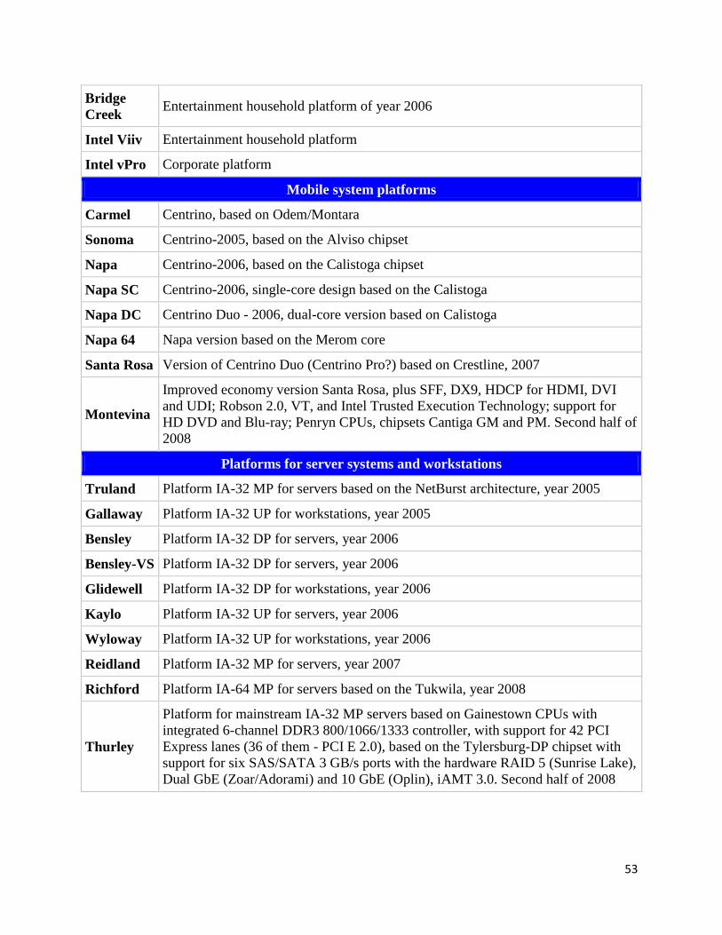
53
Bridge
Creek Entertainment household platform of year 2006
Intel Viiv Entertainment household platform
Intel vPro Corporate platform
Mobile system platforms
Carmel Centrino, based on Odem/Montara
Sonoma Centrino-2005, based on the Alviso chipset
Napa Centrino-2006, based on the Calistoga chipset
Napa SC Centrino-2006, single-core design based on the Calistoga
Napa DC Centrino Duo - 2006, dual-core version based on Calistoga
Napa 64 Napa version based on the Merom core
Santa Rosa Version of Centrino Duo (Centrino Pro?) based on Crestline, 2007
Montevina
Improved economy version Santa Rosa, plus SFF, DX9, HDCP for HDMI, DVI
and UDI; Robson 2.0, VT, and Intel Trusted Execution Technology; support for
HD DVD and Blu-ray; Penryn CPUs, chipsets Cantiga GM and PM. Second half of
2008
Platforms for server systems and workstations
Truland Platform IA-32 MP for servers based on the NetBurst architecture, year 2005
Gallaway Platform IA-32 UP for workstations, year 2005
Bensley Platform IA-32 DP for servers, year 2006
Bensley-VS Platform IA-32 DP for servers, year 2006
Glidewell Platform IA-32 DP for workstations, year 2006
Kaylo Platform IA-32 UP for servers, year 2006
Wyloway Platform IA-32 UP for workstations, year 2006
Reidland Platform IA-32 MP for servers, year 2007
Richford Platform IA-64 MP for servers based on the Tukwila, year 2008
Thurley
Platform for mainstream IA-32 MP servers based on Gainestown CPUs with
integrated 6-channel DDR3 800/1066/1333 controller, with support for 42 PCI
Express lanes (36 of them - PCI E 2.0), based on the Tylersburg-DP chipset with
support for six SAS/SATA 3 GB/s ports with the hardware RAID 5 (Sunrise Lake),
Dual GbE (Zoar/Adorami) and 10 GbE (Oplin), iAMT 3.0. Second half of 2008
54
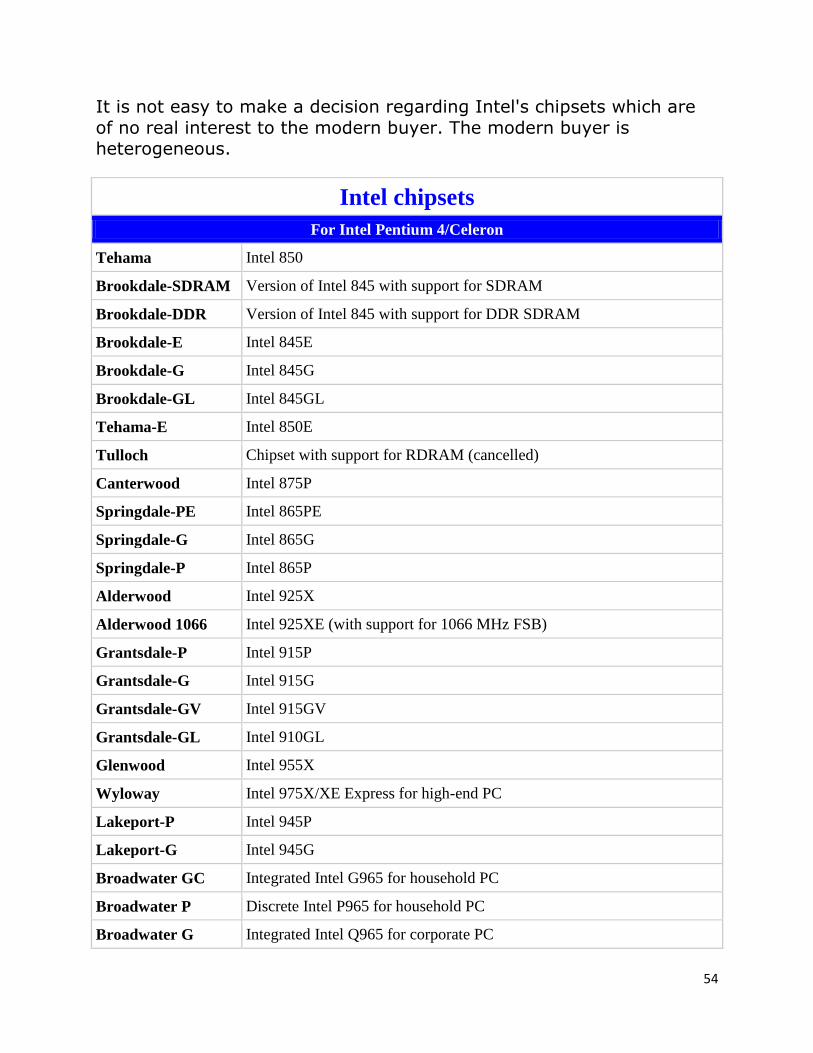
It is not easy to make a decision regarding Intel's chipsets which are
of no real interest to the modern buyer. The modern buyer is heterogeneous.
Intel chipsets
For Intel Pentium 4/Celeron
Tehama Intel 850
Brookdale-SDRAM Version of Intel 845 with support for SDRAM
Brookdale-DDR Version of Intel 845 with support for DDR SDRAM
Brookdale-E Intel 845E
Brookdale-G Intel 845G
Brookdale-GL Intel 845GL
Tehama-E Intel 850E
Tulloch Chipset with support for RDRAM (cancelled)
Canterwood Intel 875P
Springdale-PE Intel 865PE
Springdale-G Intel 865G
Springdale-P Intel 865P
Alderwood Intel 925X
Alderwood 1066 Intel 925XE (with support for 1066 MHz FSB)
Grantsdale-P Intel 915P
Grantsdale-G Intel 915G
Grantsdale-GV Intel 915GV
Grantsdale-GL Intel 910GL
Glenwood Intel 955X
Wyloway Intel 975X/XE Express for high-end PC
Lakeport-P Intel 945P
Lakeport-G Intel 945G
Broadwater GC Integrated Intel G965 for household PC
Broadwater P Discrete Intel P965 for household PC
Broadwater G Integrated Intel Q965 for corporate PC
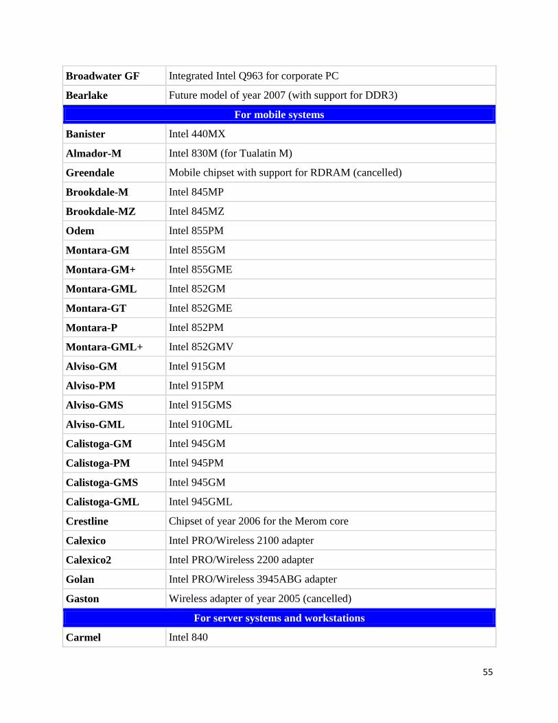
55
Broadwater GF Integrated Intel Q963 for corporate PC
Bearlake Future model of year 2007 (with support for DDR3)
For mobile systems
Banister Intel 440MX
Almador-M Intel 830M (for Tualatin M)
Greendale Mobile chipset with support for RDRAM (cancelled)
Brookdale-M Intel 845MP
Brookdale-MZ Intel 845MZ
Odem Intel 855PM
Montara-GM Intel 855GM
Montara-GM+ Intel 855GME
Montara-GML Intel 852GM
Montara-GT Intel 852GME
Montara-P Intel 852PM
Montara-GML+ Intel 852GMV
Alviso-GM Intel 915GM
Alviso-PM Intel 915PM
Alviso-GMS Intel 915GMS
Alviso-GML Intel 910GML
Calistoga-GM Intel 945GM
Calistoga-PM Intel 945PM
Calistoga-GMS Intel 945GM
Calistoga-GML Intel 945GML
Crestline Chipset of year 2006 for the Merom core
Calexico Intel PRO/Wireless 2100 adapter
Calexico2 Intel PRO/Wireless 2200 adapter
Golan Intel PRO/Wireless 3945ABG adapter
Gaston Wireless adapter of year 2005 (cancelled)
For server systems and workstations
Carmel Intel 840
56
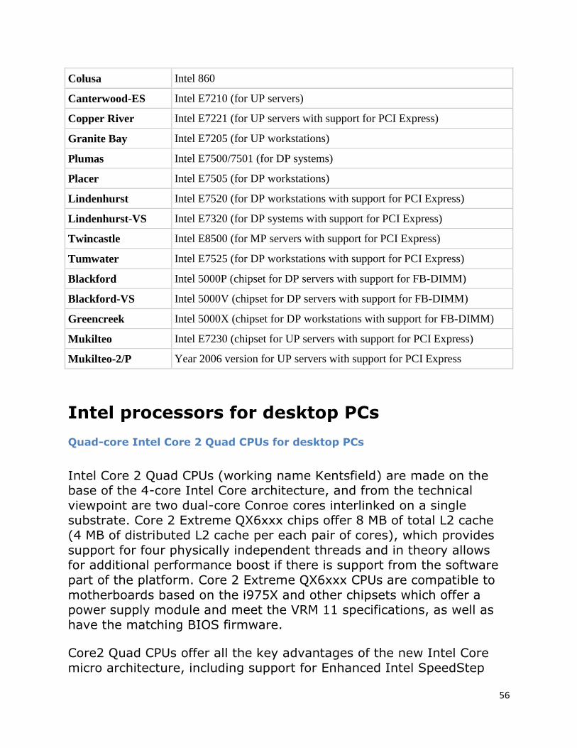
Colusa Intel 860
Canterwood-ES Intel E7210 (for UP servers)
Copper River Intel E7221 (for UP servers with support for PCI Express)
Granite Bay Intel E7205 (for UP workstations)
Plumas Intel E7500/7501 (for DP systems)
Placer Intel E7505 (for DP workstations)
Lindenhurst Intel E7520 (for DP workstations with support for PCI Express)
Lindenhurst-VS Intel E7320 (for DP systems with support for PCI Express)
Twincastle Intel E8500 (for MP servers with support for PCI Express)
Tumwater Intel E7525 (for DP workstations with support for PCI Express)
Blackford Intel 5000P (chipset for DP servers with support for FB-DIMM)
Blackford-VS Intel 5000V (chipset for DP servers with support for FB-DIMM)
Greencreek Intel 5000X (chipset for DP workstations with support for FB-DIMM)
Mukilteo Intel E7230 (chipset for UP servers with support for PCI Express)
Mukilteo-2/P Year 2006 version for UP servers with support for PCI Express
Intel processors for desktop PCs
Quad-core Intel Core 2 Quad CPUs for desktop PCs
Intel Core 2 Quad CPUs (working name Kentsfield) are made on the base of the 4-core Intel Core architecture, and from the technical
viewpoint are two dual-core Conroe cores interlinked on a single substrate. Core 2 Extreme QX6xxx chips offer 8 MB of total L2 cache
(4 MB of distributed L2 cache per each pair of cores), which provides
support for four physically independent threads and in theory allows for additional performance boost if there is support from the software
part of the platform. Core 2 Extreme QX6xxx CPUs are compatible to
motherboards based on the i975X and other chipsets which offer a power supply module and meet the VRM 11 specifications, as well as
have the matching BIOS firmware.
Core2 Quad CPUs offer all the key advantages of the new Intel Core
micro architecture, including support for Enhanced Intel SpeedStep
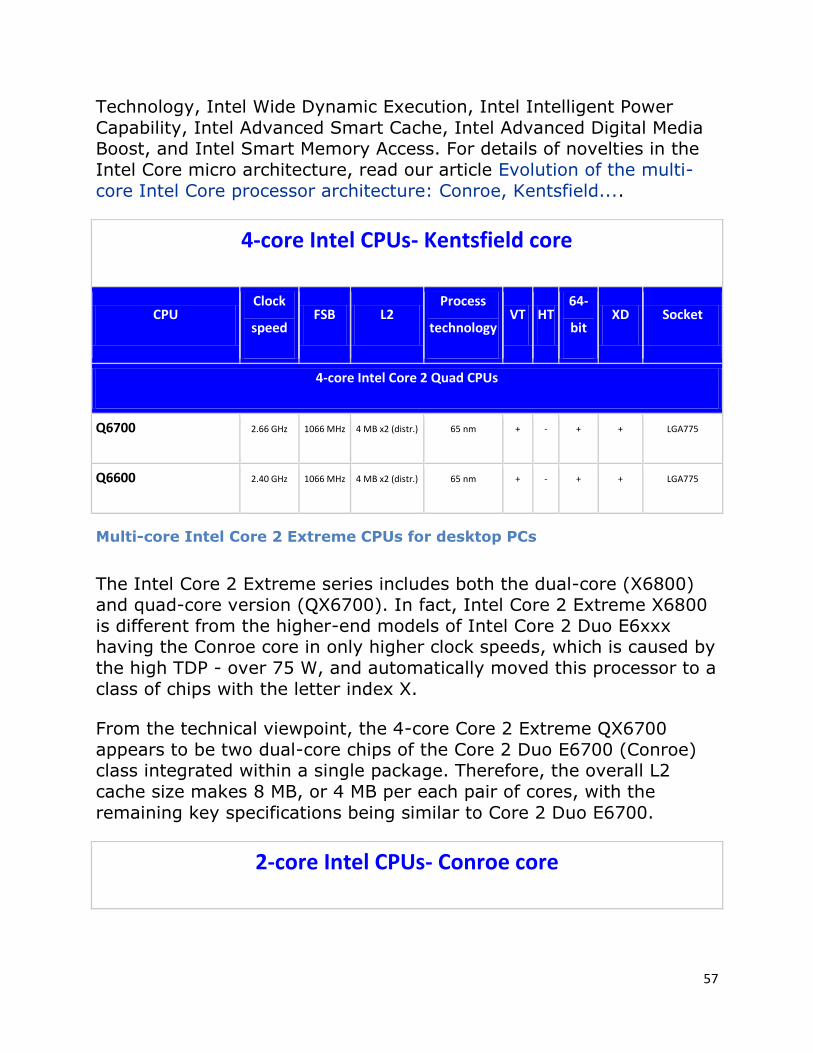
57
Technology, Intel Wide Dynamic Execution, Intel Intelligent Power
Capability, Intel Advanced Smart Cache, Intel Advanced Digital Media Boost, and Intel Smart Memory Access. For details of novelties in the
Intel Core micro architecture, read our article Evolution of the multi-
core Intel Core processor architecture: Conroe, Kentsfield....
4-core Intel CPUs- Kentsfield core
CPU Clock
speed FSB L2
Process
technology VT HT
64-
bit XD Socket
4-core Intel Core 2 Quad CPUs
Q6700 2.66 GHz 1066 MHz 4 MB х2 (distr.) 65 nm + - + + LGA775
Q6600 2.40 GHz 1066 MHz 4 MB х2 (distr.) 65 nm + - + + LGA775
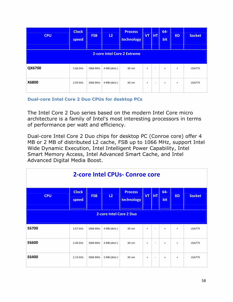
Multi-core Intel Core 2 Extreme CPUs for desktop PCs
The Intel Core 2 Extreme series includes both the dual-core (X6800) and quad-core version (QX6700). In fact, Intel Core 2 Extreme X6800
is different from the higher-end models of Intel Core 2 Duo E6xxx having the Conroe core in only higher clock speeds, which is caused by
the high TDP - over 75 W, and automatically moved this processor to a
class of chips with the letter index X.
From the technical viewpoint, the 4-core Core 2 Extreme QX6700
appears to be two dual-core chips of the Core 2 Duo E6700 (Conroe) class integrated within a single package. Therefore, the overall L2
cache size makes 8 MB, or 4 MB per each pair of cores, with the
remaining key specifications being similar to Core 2 Duo E6700.
2-core Intel CPUs- Conroe core
58
CPU Clock
speed FSB L2
Process
technology VT HT
64-
bit XD Socket
2-core Intel Core 2 Extreme
QX6700 2.66 GHz 1066 MHz 4 MB (distr.) 65 nm + - + + LGA775
X6800 2.93 GHz 1066 MHz 4 MB (distr.) 65 nm + - + + LGA775
Dual-core Intel Core 2 Duo CPUs for desktop PCs
The Intel Core 2 Duo series based on the modern Intel Core micro architecture is a family of Intel's most interesting processors in terms
of performance per watt and efficiency.
Dual-core Intel Core 2 Duo chips for desktop PC (Conroe core) offer 4
MB or 2 MB of distributed L2 cache, FSB up to 1066 MHz, support Intel
Wide Dynamic Execution, Intel Intelligent Power Capability, Intel Smart Memory Access, Intel Advanced Smart Cache, and Intel
Advanced Digital Media Boost.
2-core Intel CPUs- Conroe core
CPU Clock
speed FSB L2
Process
technology VT HT
64-
bit XD Socket
2-core Intel Core 2 Duo
E6700 2.67 GHz 1066 MHz 4 MB (distr.) 65 nm + - + + LGA775
E6600 2.40 GHz 1066 MHz 4 MB (distr.) 65 nm + - + + LGA775
E6400 2.13 GHz 1066 MHz 2 MB (distr.) 65 nm + - + + LGA775
59
E6300 1.86 GHz 1066 MHz 2 MB (distr.) 65 nm + - + + LGA775
E4300 1.80 GHz 800 MHz 2 MB (distr.) 65 nm - - + + LGA775
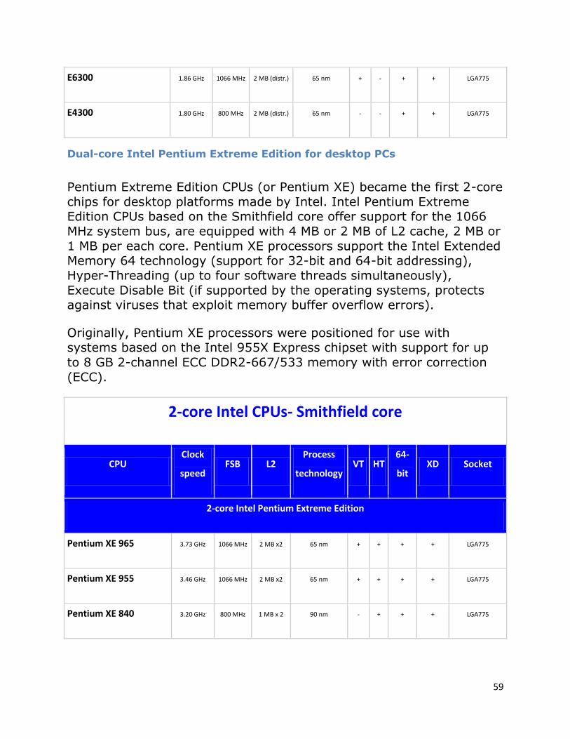
Dual-core Intel Pentium Extreme Edition for desktop PCs
Pentium Extreme Edition CPUs (or Pentium XE) became the first 2-core
chips for desktop platforms made by Intel. Intel Pentium Extreme Edition CPUs based on the Smithfield core offer support for the 1066
MHz system bus, are equipped with 4 MB or 2 MB of L2 cache, 2 MB or
1 MB per each core. Pentium XE processors support the Intel Extended Memory 64 technology (support for 32-bit and 64-bit addressing),
Hyper-Threading (up to four software threads simultaneously),
Execute Disable Bit (if supported by the operating systems, protects against viruses that exploit memory buffer overflow errors).
Originally, Pentium XE processors were positioned for use with systems based on the Intel 955X Express chipset with support for up
to 8 GB 2-channel ECC DDR2-667/533 memory with error correction
(ECC).
2-core Intel CPUs- Smithfield core
CPU Clock
speed FSB L2
Process
technology VT HT
64-
bit XD Socket
2-core Intel Pentium Extreme Edition
Pentium XE 965 3.73 GHz 1066 MHz 2 MB х2 65 nm + + + + LGA775
Pentium XE 955 3.46 GHz 1066 MHz 2 MB х2 65 nm + + + + LGA775
Pentium XE 840 3.20 GHz 800 MHz 1 MB х 2 90 nm - + + + LGA775
60
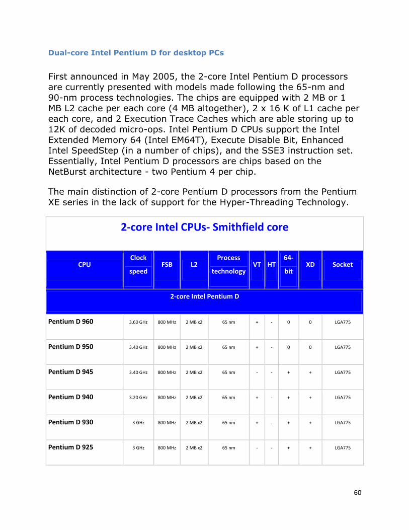
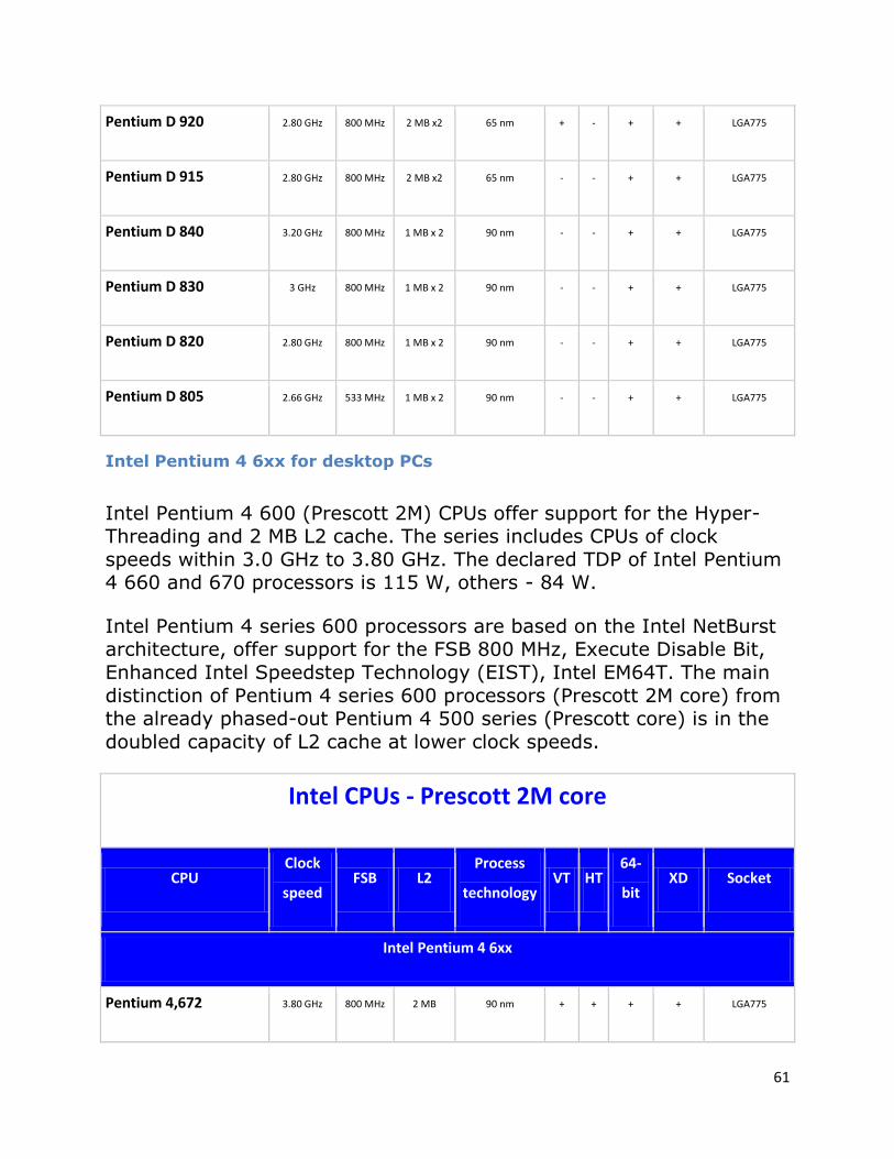
Dual-core Intel Pentium D for desktop PCs
First announced in May 2005, the 2-core Intel Pentium D processors are currently presented with models made following the 65-nm and
90-nm process technologies. The chips are equipped with 2 MB or 1
MB L2 cache per each core (4 MB altogether), 2 х 16 K of L1 cache per each core, and 2 Execution Trace Caches which are able storing up to
12K of decoded micro-ops. Intel Pentium D CPUs support the Intel
Extended Memory 64 (Intel EM64T), Execute Disable Bit, Enhanced Intel SpeedStep (in a number of chips), and the SSE3 instruction set.
Essentially, Intel Pentium D processors are chips based on the
NetBurst architecture - two Pentium 4 per chip.
The main distinction of 2-core Pentium D processors from the Pentium
XE series in the lack of support for the Hyper-Threading Technology.
2-core Intel CPUs- Smithfield core
CPU Clock
speed FSB L2
Process
technology VT HT
64-
bit XD Socket
2-core Intel Pentium D
Pentium D 960 3.60 GHz 800 MHz 2 MB х2 65 nm + - 0 0 LGA775
Pentium D 950 3.40 GHz 800 MHz 2 MB х2 65 nm + - 0 0 LGA775
Pentium D 945 3.40 GHz 800 MHz 2 MB х2 65 nm - - + + LGA775
Pentium D 940 3.20 GHz 800 MHz 2 MB х2 65 nm + - + + LGA775
Pentium D 930 3 GHz 800 MHz 2 MB х2 65 nm + - + + LGA775
Pentium D 925 3 GHz 800 MHz 2 MB х2 65 nm - - + + LGA775
61
Pentium D 920 2.80 GHz 800 MHz 2 MB х2 65 nm + - + + LGA775
Pentium D 915 2.80 GHz 800 MHz 2 MB х2 65 nm - - + + LGA775
Pentium D 840 3.20 GHz 800 MHz 1 MB х 2 90 nm - - + + LGA775
Pentium D 830 3 GHz 800 MHz 1 MB х 2 90 nm - - + + LGA775
Pentium D 820 2.80 GHz 800 MHz 1 MB х 2 90 nm - - + + LGA775
Pentium D 805 2.66 GHz 533 MHz 1 MB х 2 90 nm - - + + LGA775
Intel Pentium 4 6xx for desktop PCs
Intel Pentium 4 600 (Prescott 2M) CPUs offer support for the Hyper-Threading and 2 MB L2 cache. The series includes CPUs of clock
speeds within 3.0 GHz to 3.80 GHz. The declared TDP of Intel Pentium 4 660 and 670 processors is 115 W, others - 84 W.
Intel Pentium 4 series 600 processors are based on the Intel NetBurst architecture, offer support for the FSB 800 MHz, Execute Disable Bit,
Enhanced Intel Speedstep Technology (EIST), Intel EM64T. The main
distinction of Pentium 4 series 600 processors (Prescott 2M core) from the already phased-out Pentium 4 500 series (Prescott core) is in the
doubled capacity of L2 cache at lower clock speeds.
Intel CPUs - Prescott 2M core
CPU Clock
speed FSB L2
Process
technology VT HT
64-
bit XD Socket
Intel Pentium 4 6xx
Pentium 4,672 3.80 GHz 800 MHz 2 MB 90 nm + + + + LGA775
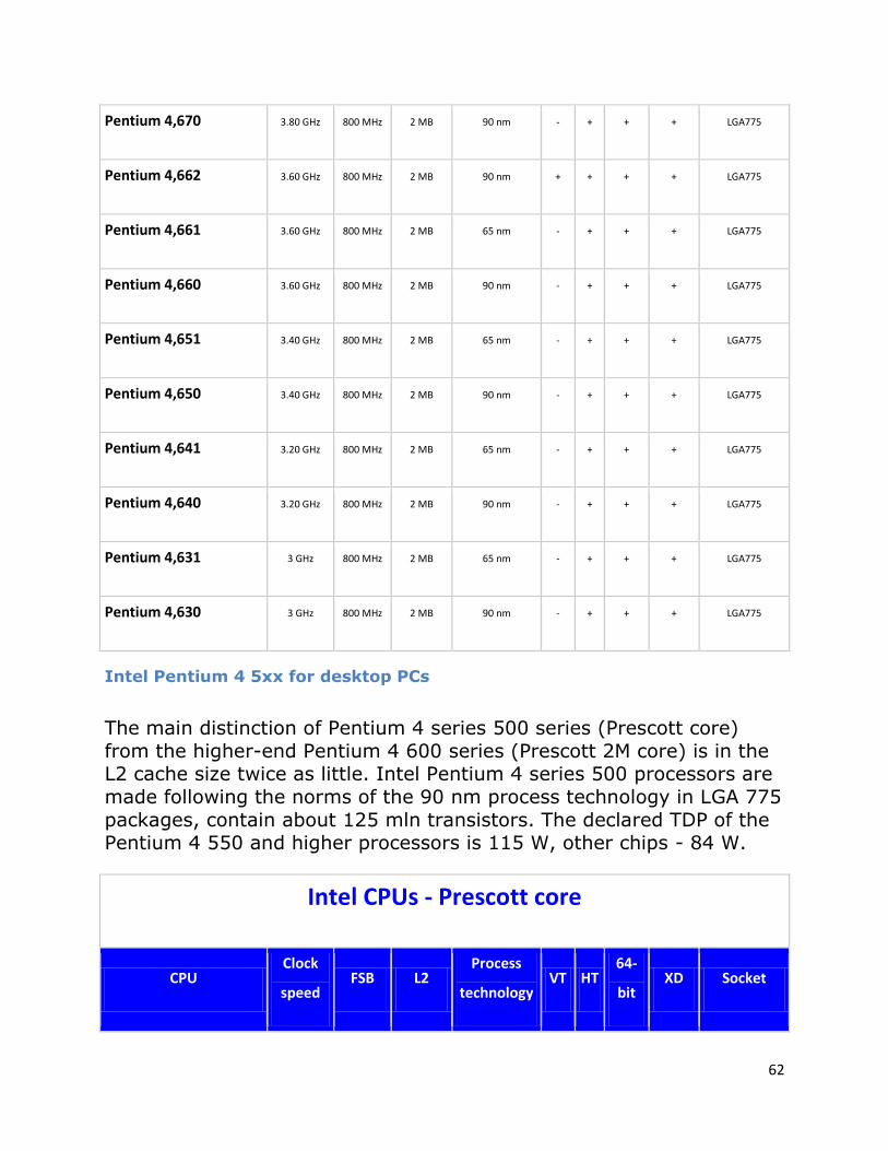
62
Pentium 4,670 3.80 GHz 800 MHz 2 MB 90 nm - + + + LGA775
Pentium 4,662 3.60 GHz 800 MHz 2 MB 90 nm + + + + LGA775
Pentium 4,661 3.60 GHz 800 MHz 2 MB 65 nm - + + + LGA775
Pentium 4,660 3.60 GHz 800 MHz 2 MB 90 nm - + + + LGA775
Pentium 4,651 3.40 GHz 800 MHz 2 MB 65 nm - + + + LGA775
Pentium 4,650 3.40 GHz 800 MHz 2 MB 90 nm - + + + LGA775
Pentium 4,641 3.20 GHz 800 MHz 2 MB 65 nm - + + + LGA775
Pentium 4,640 3.20 GHz 800 MHz 2 MB 90 nm - + + + LGA775
Pentium 4,631 3 GHz 800 MHz 2 MB 65 nm - + + + LGA775
Pentium 4,630 3 GHz 800 MHz 2 MB 90 nm - + + + LGA775
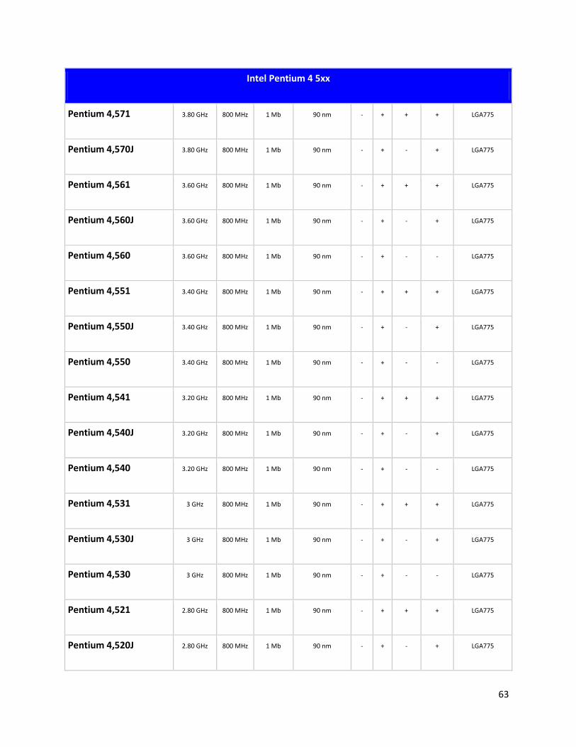
Intel Pentium 4 5xx for desktop PCs
The main distinction of Pentium 4 series 500 series (Prescott core)
from the higher-end Pentium 4 600 series (Prescott 2M core) is in the L2 cache size twice as little. Intel Pentium 4 series 500 processors are
made following the norms of the 90 nm process technology in LGA 775
packages, contain about 125 mln transistors. The declared TDP of the Pentium 4 550 and higher processors is 115 W, other chips - 84 W.
Intel CPUs - Prescott core
CPU Clock
speed FSB L2
Process
technology VT HT
64-
bit XD Socket
63
Intel Pentium 4 5xx
Pentium 4,571 3.80 GHz 800 MHz 1 Mb 90 nm - + + + LGA775
Pentium 4,570J 3.80 GHz 800 MHz 1 Mb 90 nm - + - + LGA775
Pentium 4,561 3.60 GHz 800 MHz 1 Mb 90 nm - + + + LGA775
Pentium 4,560J 3.60 GHz 800 MHz 1 Mb 90 nm - + - + LGA775
Pentium 4,560 3.60 GHz 800 MHz 1 Mb 90 nm - + - - LGA775
Pentium 4,551 3.40 GHz 800 MHz 1 Mb 90 nm - + + + LGA775
Pentium 4,550J 3.40 GHz 800 MHz 1 Mb 90 nm - + - + LGA775
Pentium 4,550 3.40 GHz 800 MHz 1 Mb 90 nm - + - - LGA775
Pentium 4,541 3.20 GHz 800 MHz 1 Mb 90 nm - + + + LGA775
Pentium 4,540J 3.20 GHz 800 MHz 1 Mb 90 nm - + - + LGA775
Pentium 4,540 3.20 GHz 800 MHz 1 Mb 90 nm - + - - LGA775
Pentium 4,531 3 GHz 800 MHz 1 Mb 90 nm - + + + LGA775
Pentium 4,530J 3 GHz 800 MHz 1 Mb 90 nm - + - + LGA775
Pentium 4,530 3 GHz 800 MHz 1 Mb 90 nm - + - - LGA775
Pentium 4,521 2.80 GHz 800 MHz 1 Mb 90 nm - + + + LGA775
Pentium 4,520J 2.80 GHz 800 MHz 1 Mb 90 nm - + - + LGA775
64
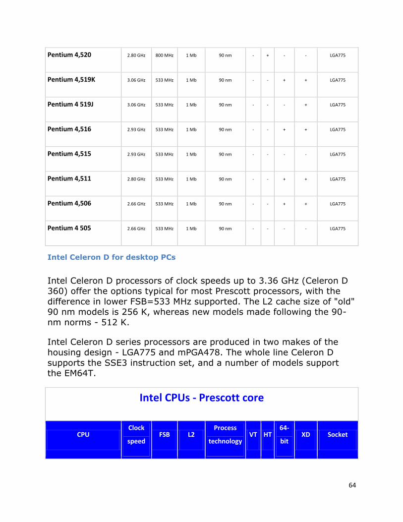
Pentium 4,520 2.80 GHz 800 MHz 1 Mb 90 nm - + - - LGA775
Pentium 4,519K 3.06 GHz 533 MHz 1 Mb 90 nm - - + + LGA775
Pentium 4 519J 3.06 GHz 533 MHz 1 Mb 90 nm - - - + LGA775
Pentium 4,516 2.93 GHz 533 MHz 1 Mb 90 nm - - + + LGA775
Pentium 4,515 2.93 GHz 533 MHz 1 Mb 90 nm - - - - LGA775
Pentium 4,511 2.80 GHz 533 MHz 1 Mb 90 nm - - + + LGA775
Pentium 4,506 2.66 GHz 533 MHz 1 Mb 90 nm - - + + LGA775
Pentium 4 505 2.66 GHz 533 MHz 1 Mb 90 nm - - - - LGA775
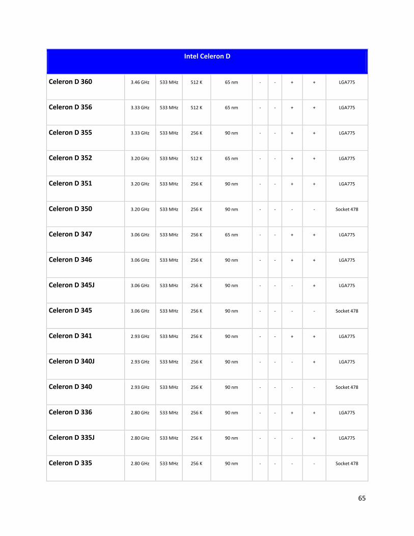
Intel Celeron D for desktop PCs
Intel Celeron D processors of clock speeds up to 3.36 GHz (Celeron D 360) offer the options typical for most Prescott processors, with the
difference in lower FSB=533 MHz supported. The L2 cache size of "old" 90 nm models is 256 K, whereas new models made following the 90-
nm norms - 512 K.
Intel Celeron D series processors are produced in two makes of the
housing design - LGA775 and mPGA478. The whole line Celeron D
supports the SSE3 instruction set, and a number of models support the EM64T.
Intel CPUs - Prescott core
CPU Clock
speed FSB L2
Process
technology VT HT
64-
bit XD Socket
65
Intel Celeron D
Celeron D 360 3.46 GHz 533 MHz 512 K 65 nm - - + + LGA775
Celeron D 356 3.33 GHz 533 MHz 512 K 65 nm - - + + LGA775
Celeron D 355 3.33 GHz 533 MHz 256 K 90 nm - - + + LGA775
Celeron D 352 3.20 GHz 533 MHz 512 K 65 nm - - + + LGA775
Celeron D 351 3.20 GHz 533 MHz 256 K 90 nm - - + + LGA775
Celeron D 350 3.20 GHz 533 MHz 256 K 90 nm - - - - Socket 478
Celeron D 347 3.06 GHz 533 MHz 256 K 65 nm - - + + LGA775
Celeron D 346 3.06 GHz 533 MHz 256 K 90 nm - - + + LGA775
Celeron D 345J 3.06 GHz 533 MHz 256 K 90 nm - - - + LGA775
Celeron D 345 3.06 GHz 533 MHz 256 K 90 nm - - - - Socket 478
Celeron D 341 2.93 GHz 533 MHz 256 K 90 nm - - + + LGA775
Celeron D 340J 2.93 GHz 533 MHz 256 K 90 nm - - - + LGA775
Celeron D 340 2.93 GHz 533 MHz 256 K 90 nm - - - - Socket 478
Celeron D 336 2.80 GHz 533 MHz 256 K 90 nm - - + + LGA775
Celeron D 335J 2.80 GHz 533 MHz 256 K 90 nm - - - + LGA775
Celeron D 335 2.80 GHz 533 MHz 256 K 90 nm - - - - Socket 478
66
Celeron D 331 2.66 GHz 533 MHz 256 K 90 nm - - + + LGA775
Celeron D 330J 2.66 GHz 533 MHz 256 K 90 nm - - - + LGA775
Celeron D 330 2.66 GHz 533 MHz 256 K 90 nm - - - - Socket 478
Celeron D 326 2.53 GHz 533 MHz 256 K 90 nm - - + + LGA775
Celeron D 325J 2.53 GHz 533 MHz 256 K 90 nm - - - + LGA775
Celeron D 325 2.53 GHz 533 MHz 256 K 90 nm - - - - Socket 478
Celeron D 320 2.40 GHz 533 MHz 256 K 90 nm - - - - Socket 478
Celeron D 315 2.26 GHz 533 MHz 256 K 90 nm - - - - Socket 478
Celeron D 310 2.13 GHz 533 MHz 256 K 90 nm - - - - Socket 478
Intel CPUs for mobile and compact PCs
Intel processors for mobile PCs - Pentium M or Celeron M - are inseparably linked with the integrated Centrino platform for mobile PCs
promoted by the company for several years, which includes Intel's
best technologies for notebook PCs.
Dual-core Intel Core 2 Duo CPUs for mobile and compact PCs
From a certain time, the new Intel Core architecture has been topical for all the market sectors - mobile, desktop, and server systems.
Having inherited the philosophy of efficient power consumption first
implemented in Intel Pentium M for mobile PCs with the working name Banias, owing to new technologies and implementation of some
developments of the new NetBurst architecture, the new generation
67
architecture has improved the ratings. Here are the key innovations of
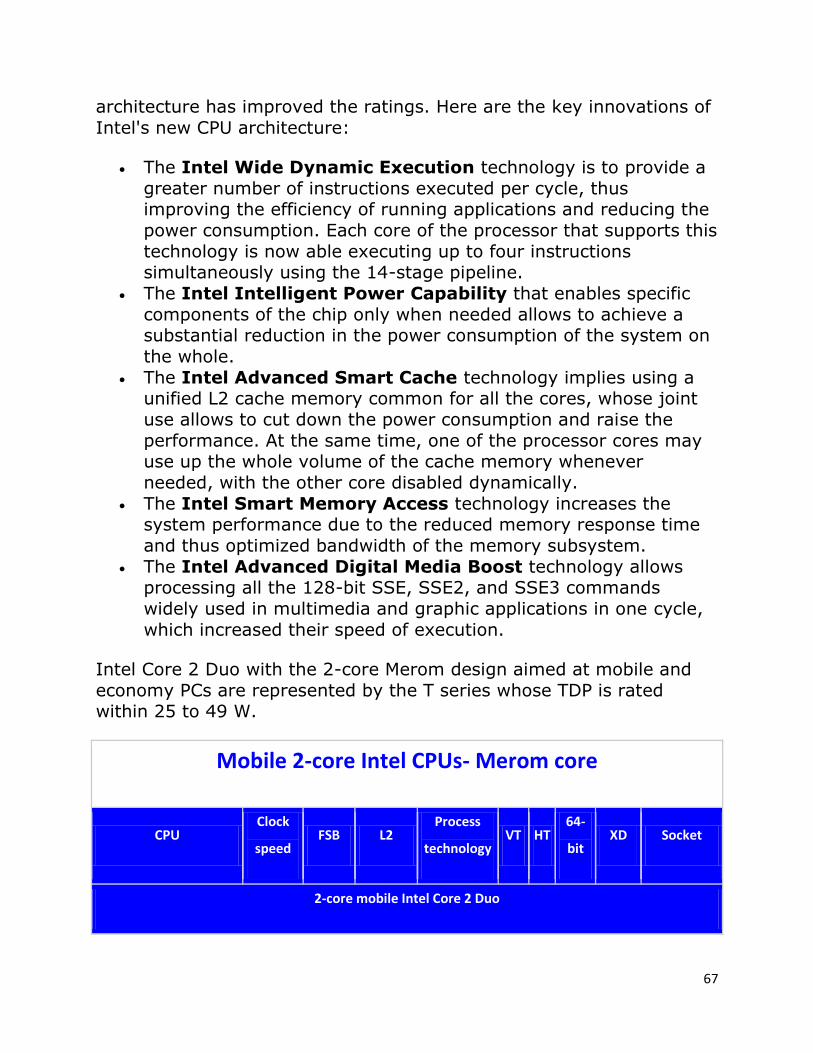
Intel's new CPU architecture:
The Intel Wide Dynamic Execution technology is to provide a
greater number of instructions executed per cycle, thus improving the efficiency of running applications and reducing the
power consumption. Each core of the processor that supports this
technology is now able executing up to four instructions simultaneously using the 14-stage pipeline.
The Intel Intelligent Power Capability that enables specific
components of the chip only when needed allows to achieve a substantial reduction in the power consumption of the system on
the whole.
The Intel Advanced Smart Cache technology implies using a unified L2 cache memory common for all the cores, whose joint
use allows to cut down the power consumption and raise the
performance. At the same time, one of the processor cores may use up the whole volume of the cache memory whenever
needed, with the other core disabled dynamically.
The Intel Smart Memory Access technology increases the system performance due to the reduced memory response time
and thus optimized bandwidth of the memory subsystem.
The Intel Advanced Digital Media Boost technology allows processing all the 128-bit SSE, SSE2, and SSE3 commands
widely used in multimedia and graphic applications in one cycle,
which increased their speed of execution.
Intel Core 2 Duo with the 2-core Merom design aimed at mobile and
economy PCs are represented by the Т series whose TDP is rated within 25 to 49 W.
Mobile 2-core Intel CPUs- Merom core
CPU Clock
speed FSB L2
Process
technology VT HT
64-
bit XD Socket
2-core mobile Intel Core 2 Duo
68
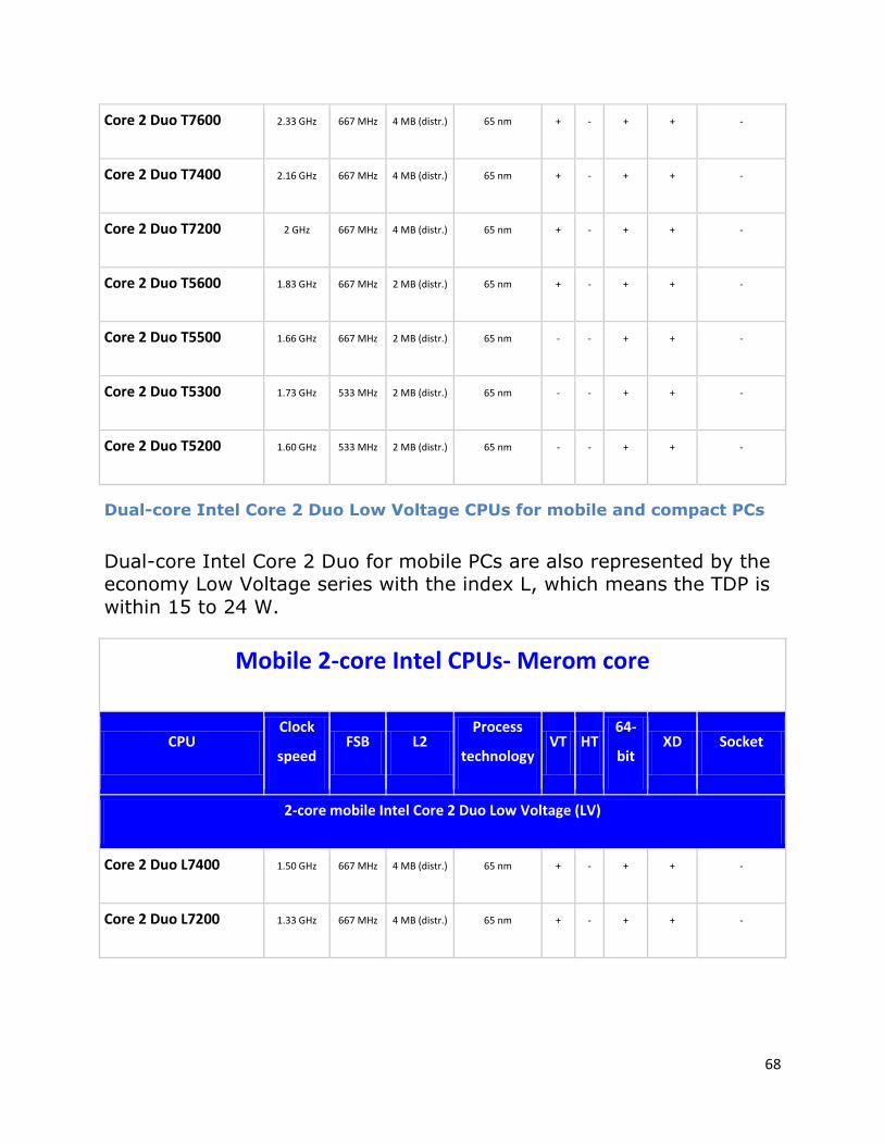
Core 2 Duo T7600 2.33 GHz 667 MHz 4 MB (distr.) 65 nm + - + + -
Core 2 Duo T7400 2.16 GHz 667 MHz 4 MB (distr.) 65 nm + - + + -
Core 2 Duo T7200 2 GHz 667 MHz 4 MB (distr.) 65 nm + - + + -
Core 2 Duo T5600 1.83 GHz 667 MHz 2 MB (distr.) 65 nm + - + + -
Core 2 Duo T5500 1.66 GHz 667 MHz 2 MB (distr.) 65 nm - - + + -
Core 2 Duo T5300 1.73 GHz 533 MHz 2 MB (distr.) 65 nm - - + + -
Core 2 Duo T5200 1.60 GHz 533 MHz 2 MB (distr.) 65 nm - - + + -
Dual-core Intel Core 2 Duo Low Voltage CPUs for mobile and compact PCs
Dual-core Intel Core 2 Duo for mobile PCs are also represented by the economy Low Voltage series with the index L, which means the TDP is
within 15 to 24 W.
Mobile 2-core Intel CPUs- Merom core
CPU Clock
speed FSB L2
Process
technology VT HT
64-
bit XD Socket
2-core mobile Intel Core 2 Duo Low Voltage (LV)
Core 2 Duo L7400 1.50 GHz 667 MHz 4 MB (distr.) 65 nm + - + + -
Core 2 Duo L7200 1.33 GHz 667 MHz 4 MB (distr.) 65 nm + - + + -
69
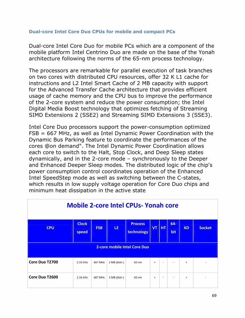
Dual-core Intel Core Duo CPUs for mobile and compact PCs
Dual-core Intel Core Duo for mobile PCs which are a component of the mobile platform Intel Centrino Duo are made on the base of the Yonah
architecture following the norms of the 65-nm process technology.
The processors are remarkable for parallel execution of task branches
on two cores with distributed CPU resources, offer 32 K L1 cache for
instructions and L2 Intel Smart Cache of 2 MB capacity with support for the Advanced Transfer Cache architecture that provides efficient
usage of cache memory and the CPU bus to improve the performance
of the 2-core system and reduce the power consumption; the Intel
Digital Media Boost technology that optimizes fetching of Streaming
SIMD Extensions 2 (SSE2) and Streaming SIMD Extensions 3 (SSE3).
Intel Core Duo processors support the power-consumption optimized
FSB = 667 MHz, as well as Intel Dynamic Power Coordination with the
Dynamic Bus Parking feature to coordinate the performances of the cores @on demand". The Intel Dynamic Power Coordination allows
each core to switch to the Halt, Stop Clock, and Deep Sleep states
dynamically, and in the 2-core mode – synchronously to the Deeper and Enhanced Deeper Sleep modes. The distributed logic of the chip's
power consumption control coordinates operation of the Enhanced
Intel SpeedStep mode as well as switching between the C-states, which results in low supply voltage operation for Core Duo chips and
minimum heat dissipation in the active state
Mobile 2-core Intel CPUs- Yonah core
CPU Clock
speed FSB L2
Process
technology VT HT
64-
bit XD Socket
2-core mobile Intel Core Duo
Core Duo T2700 2.33 GHz 667 MHz 2 MB (distr.) 65 nm + - - + -
Core Duo T2600 2.16 GHz 667 MHz 2 MB (distr.) 65 nm + - - + -
70
Core Duo T2500 2 GHz 667 MHz 2 MB (distr.) 65 nm + - - + -
Core Duo T2400 1.83 GHz 667 MHz 2 MB (distr.) 65 nm + - - + -
Core Duo T2300 1.66 GHz 667 MHz 2 MB (distr.) 65 nm + - - + -
Core Duo T2300E 1.66 GHz 667 MHz 2 MB (distr.) 65 nm - - - + -
Core Duo T2250 1.73 GHz 533 MHz 2 MB (distr.) 65 nm - - - + -
Core Duo T2050 1.60 GHz 533 MHz 2 MB (distr.) 65 nm - - - + -
Core Duo L2500 1.83 GHz 667 MHz 2 MB (distr.) 65 nm + - - + -
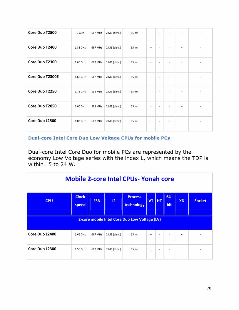
Dual-core Intel Core Duo Low Voltage CPUs for mobile PCs
Dual-core Intel Core Duo for mobile PCs are represented by the economy Low Voltage series with the index L, which means the TDP is
within 15 to 24 W.
Mobile 2-core Intel CPUs- Yonah core
CPU Clock
speed FSB L2
Process
technology VT HT
64-
bit XD Socket
2-core mobile Intel Core Duo Low Voltage (LV)
Core Duo L2400 1.66 GHz 667 MHz 2 MB (distr.) 65 nm + - - + -
Core Duo L2300 1.50 GHz 667 MHz 2 MB (distr.) 65 nm + - - + -
71
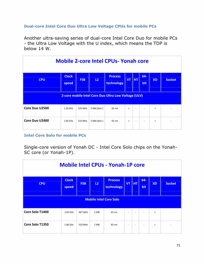
Dual-core Intel Core Duo Ultra Low Voltage CPUs for mobile PCs
Another ultra-saving series of dual-core Intel Core Duo for mobile PCs - the Ultra Low Voltage with the U index, which means the TDP is
below 14 W.
Mobile 2-core Intel CPUs- Yonah core
CPU Clock
speed FSB L2
Process
technology VT HT
64-
bit XD Socket
2-core mobile Intel Core Duo Ultra Low Voltage (ULV)
Core Duo U2500 1.20 GHz 533 MHz 2 MB (distr.) 65 nm + - - + -
Core Duo U2400 1.06 GHz 533 MHz 2 MB (distr.) 65 nm + - - + -
Intel Core Solo for mobile PCs
Single-core version of Yonah DC - Intel Core Solo chips on the Yonah-SC core (or Yonah-1P).
Mobile Intel CPUs - Yonah-1P core
CPU Clock
speed FSB L2
Process
technology VT HT
64-
bit XD Socket
Mobile Intel Core Solo
Core Solo T1400 1.83 GHz 667 MHz 2 MB 65 nm - - - + -
Core Solo T1350 1.86 GHz 533 MHz 2 MB 65 nm - - - + -
72
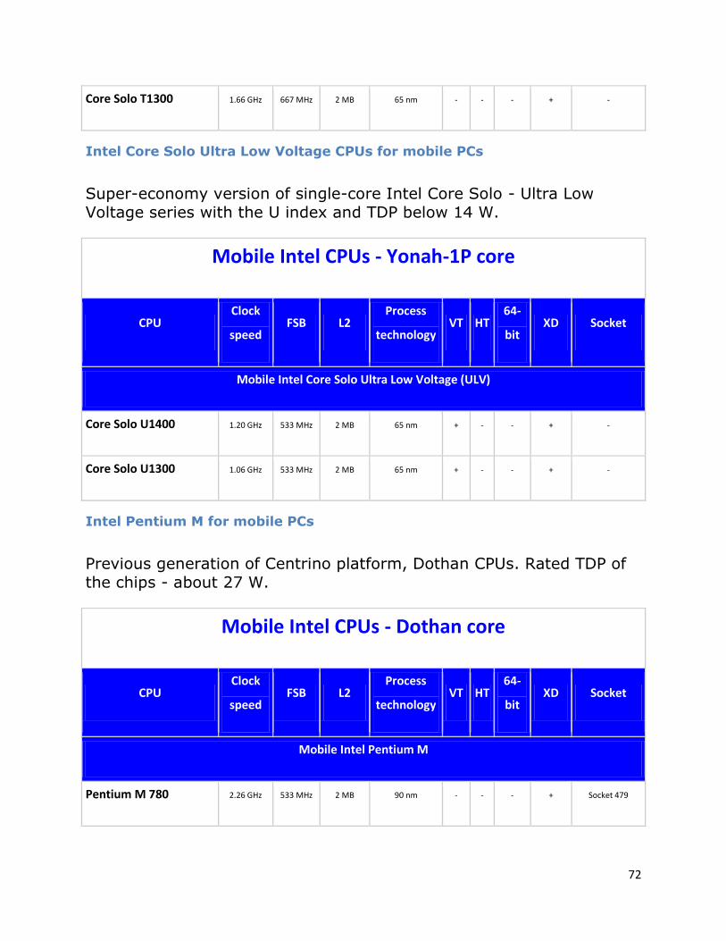
Core Solo T1300 1.66 GHz 667 MHz 2 MB 65 nm - - - + -
Intel Core Solo Ultra Low Voltage CPUs for mobile PCs
Super-economy version of single-core Intel Core Solo - Ultra Low Voltage series with the U index and TDP below 14 W.
Mobile Intel CPUs - Yonah-1P core
CPU Clock
speed FSB L2
Process
technology VT HT
64-
bit XD Socket
Mobile Intel Core Solo Ultra Low Voltage (ULV)
Core Solo U1400 1.20 GHz 533 MHz 2 MB 65 nm + - - + -
Core Solo U1300 1.06 GHz 533 MHz 2 MB 65 nm + - - + -
Intel Pentium M for mobile PCs
Previous generation of Centrino platform, Dothan CPUs. Rated TDP of the chips - about 27 W.
Mobile Intel CPUs - Dothan core
CPU Clock
speed FSB L2
Process
technology VT HT
64-
bit XD Socket
Mobile Intel Pentium M
Pentium M 780 2.26 GHz 533 MHz 2 MB 90 nm - - - + Socket 479
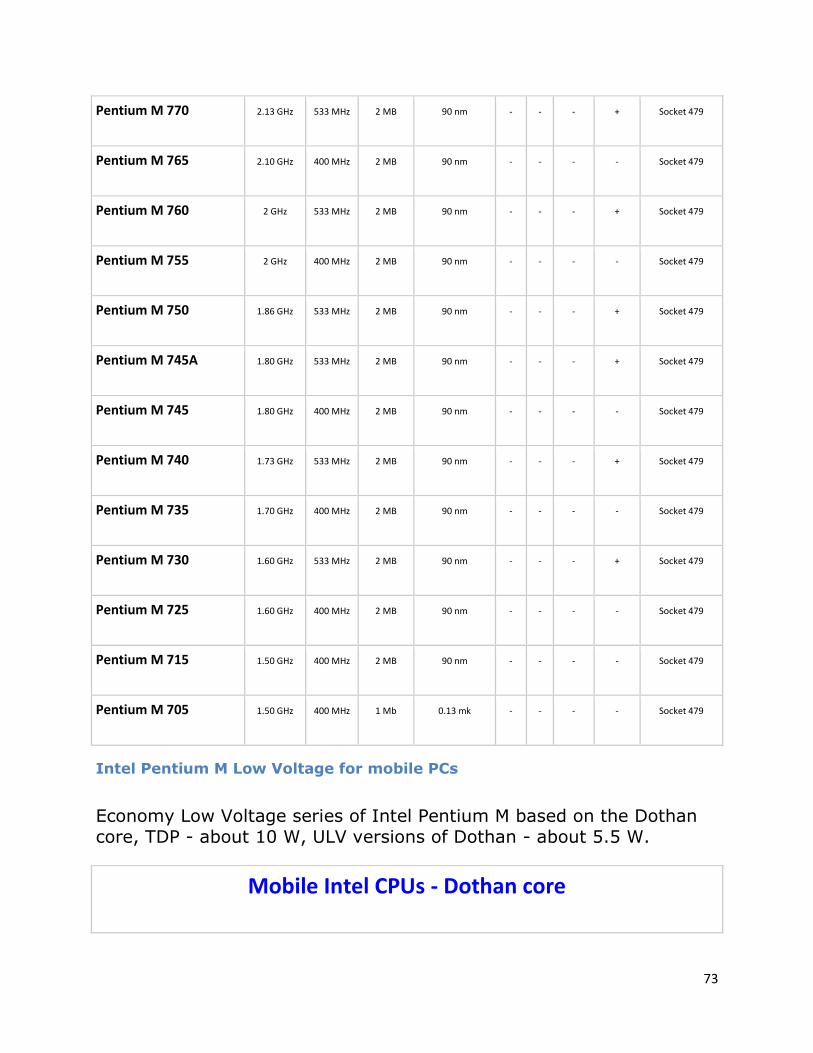
73
Pentium M 770 2.13 GHz 533 MHz 2 MB 90 nm - - - + Socket 479
Pentium M 765 2.10 GHz 400 MHz 2 MB 90 nm - - - - Socket 479
Pentium M 760 2 GHz 533 MHz 2 MB 90 nm - - - + Socket 479
Pentium M 755 2 GHz 400 MHz 2 MB 90 nm - - - - Socket 479
Pentium M 750 1.86 GHz 533 MHz 2 MB 90 nm - - - + Socket 479
Pentium M 745A 1.80 GHz 533 MHz 2 MB 90 nm - - - + Socket 479
Pentium M 745 1.80 GHz 400 MHz 2 MB 90 nm - - - - Socket 479
Pentium M 740 1.73 GHz 533 MHz 2 MB 90 nm - - - + Socket 479
Pentium M 735 1.70 GHz 400 MHz 2 MB 90 nm - - - - Socket 479
Pentium M 730 1.60 GHz 533 MHz 2 MB 90 nm - - - + Socket 479
Pentium M 725 1.60 GHz 400 MHz 2 MB 90 nm - - - - Socket 479
Pentium M 715 1.50 GHz 400 MHz 2 MB 90 nm - - - - Socket 479
Pentium M 705 1.50 GHz 400 MHz 1 Mb 0.13 mk - - - - Socket 479
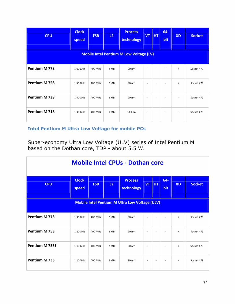
Intel Pentium M Low Voltage for mobile PCs
Economy Low Voltage series of Intel Pentium M based on the Dothan core, TDP - about 10 W, ULV versions of Dothan - about 5.5 W.
Mobile Intel CPUs - Dothan core
74
CPU Clock
speed FSB L2
Process
technology VT HT
64-
bit XD Socket
Mobile Intel Pentium M Low Voltage (LV)
Pentium M 778 1.60 GHz 400 MHz 2 MB 90 nm - - - + Socket 479
Pentium M 758 1.50 GHz 400 MHz 2 MB 90 nm - - - + Socket 479
Pentium M 738 1.40 GHz 400 MHz 2 MB 90 nm - - - - Socket 479
Pentium M 718 1.30 GHz 400 MHz 1 Mb 0.13 mk - - - - Socket 479
Intel Pentium M Ultra Low Voltage for mobile PCs
Super-economy Ultra Low Voltage (ULV) series of Intel Pentium M based on the Dothan core, TDP - about 5.5 W.
Mobile Intel CPUs - Dothan core
CPU Clock
speed FSB L2
Process
technology VT HT
64-
bit XD Socket
Mobile Intel Pentium M Ultra Low Voltage (ULV)
Pentium M 773 1.30 GHz 400 MHz 2 MB 90 nm - - - + Socket 479
Pentium M 753 1.20 GHz 400 MHz 2 MB 90 nm - - - + Socket 479
Pentium M 733J 1.10 GHz 400 MHz 2 MB 90 nm - - - + Socket 479
Pentium M 733 1.10 GHz 400 MHz 2 MB 90 nm - - - - Socket 479
75
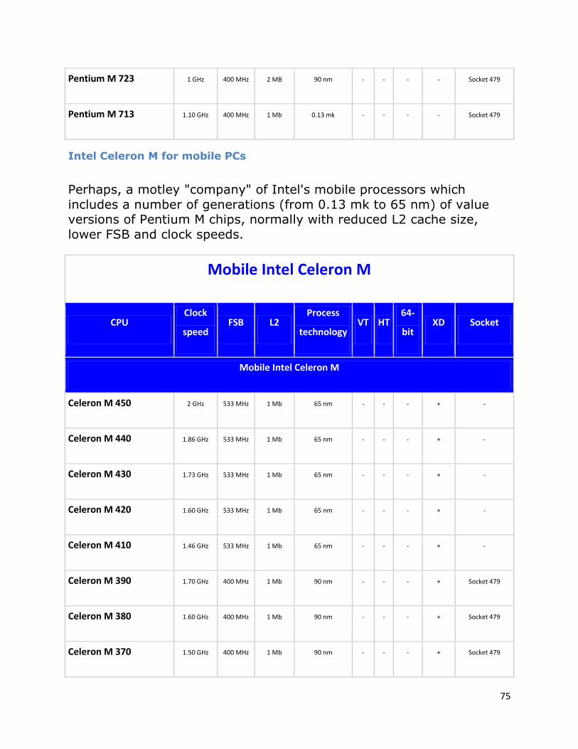
Pentium M 723 1 GHz 400 MHz 2 MB 90 nm - - - - Socket 479
Pentium M 713 1.10 GHz 400 MHz 1 Mb 0.13 mk - - - - Socket 479
Intel Celeron M for mobile PCs
Perhaps, a motley "company" of Intel's mobile processors which
includes a number of generations (from 0.13 mk to 65 nm) of value versions of Pentium M chips, normally with reduced L2 cache size,
lower FSB and clock speeds.
Mobile Intel Celeron M
CPU Clock
speed FSB L2
Process
technology VT HT
64-
bit XD Socket
Mobile Intel Celeron M
Celeron M 450 2 GHz 533 MHz 1 Mb 65 nm - - - + -
Celeron M 440 1.86 GHz 533 MHz 1 Mb 65 nm - - - + -
Celeron M 430 1.73 GHz 533 MHz 1 Mb 65 nm - - - + -
Celeron M 420 1.60 GHz 533 MHz 1 Mb 65 nm - - - + -
Celeron M 410 1.46 GHz 533 MHz 1 Mb 65 nm - - - + -
Celeron M 390 1.70 GHz 400 MHz 1 Mb 90 nm - - - + Socket 479
Celeron M 380 1.60 GHz 400 MHz 1 Mb 90 nm - - - + Socket 479
Celeron M 370 1.50 GHz 400 MHz 1 Mb 90 nm - - - + Socket 479
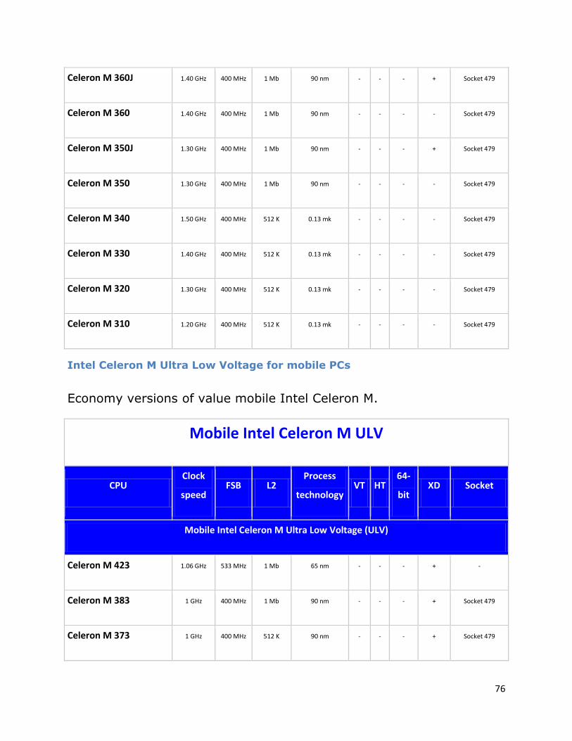
76
Celeron M 360J 1.40 GHz 400 MHz 1 Mb 90 nm - - - + Socket 479
Celeron M 360 1.40 GHz 400 MHz 1 Mb 90 nm - - - - Socket 479
Celeron M 350J 1.30 GHz 400 MHz 1 Mb 90 nm - - - + Socket 479
Celeron M 350 1.30 GHz 400 MHz 1 Mb 90 nm - - - - Socket 479
Celeron M 340 1.50 GHz 400 MHz 512 K 0.13 mk - - - - Socket 479
Celeron M 330 1.40 GHz 400 MHz 512 K 0.13 mk - - - - Socket 479
Celeron M 320 1.30 GHz 400 MHz 512 K 0.13 mk - - - - Socket 479
Celeron M 310 1.20 GHz 400 MHz 512 K 0.13 mk - - - - Socket 479
Intel Celeron M Ultra Low Voltage for mobile PCs
Economy versions of value mobile Intel Celeron M.
Mobile Intel Celeron M ULV
CPU Clock
speed FSB L2
Process
technology VT HT
64-
bit XD Socket
Mobile Intel Celeron M Ultra Low Voltage (ULV)
Celeron M 423 1.06 GHz 533 MHz 1 Mb 65 nm - - - + -
Celeron M 383 1 GHz 400 MHz 1 Mb 90 nm - - - + Socket 479
Celeron M 373 1 GHz 400 MHz 512 K 90 nm - - - + Socket 479

77
Celeron M 353 900 MHz 400 MHz 512 K 90 nm - - - - Socket 479
Celeron M 333 900 MHz 400 MHz 512 K 0.13 mk - - - - Socket 479