DESIGN CHALLENGES FOR DEEP SUBMICRON HIGH … · DESIGN CHALLENGES FOR DEEP SUBMICRON HIGH...
12
U.P.B. Sci. Bull., Series C, Vol. 70, No. 2, 2008 ISSN 1454-234x DESIGN CHALLENGES FOR DEEP SUBMICRON HIGH FREQUENCY INTEGRATED CIRCUITS Cristian M. ALBINĂ 1 Cursa continuă pentru reducerea dimensiunilor fizice în circuitele integrate este limitată în prezent de considerente fizice, tehnologice şi economice. Subiectul acestei lucrări este trecerea în revistă în primele două secţiuni a unora dintre problemele apărute datorită reducerii dimensiunilor tranzistoarelor şi a prelucrării tehnologice, precum şi a principalelor probleme întâlnite în proiectarea şi implementarea circuitelor integrate de înaltă frecvenţă. De asemenea, în ultima secţiune a lucrării vor fi prezentate câteva soluţii de implementare a circuitelor electrice în vederea minimizării efectelor parazite ale layout-ului, soluţii confirmate de-a lungul anilor în diferite circuite integrate proiectate personal şi aflate în prezent în producţie. The ultimate downsizing of the minimum feature size is hampered by physical, technological and economical limitations. To ensure Moore’s law below 100 nm technology nodes both front- and back-end processing has to face technological challenges as clearly stipulated by the International Technology Roadmap for Semiconductors (ITRS). This presentation reviews some of the on- going research efforts to come to cost-effective solutions forming the backbone for future technology generations focusing on the main aspects encountered in the high frequency circuit design and implementation. In the last section of the paper some solutions on how to implement most common modules used inside the integrated circuits will be presented. These solutions were confirmed through the years in several projects I worked to. Keywords: CMOS integrated circuits, MOSFET design, radio frequency RF, very large scale of integration VLSI 1. Introduction MOS very-large-scale-integration circuits (VLSI’s), having advanced remarkably during the past 30 years, are expected to continue to progress well into the future. The progress has been driven by the downsizing of the components in a VLSI, such as MOSFET’s. However, even before the downsizing of the VLSI devices reaches its fundamental limits this process is expected to encounter severe technological and economic problems when the minimum features of the active devices are going to shift to dimensions below 0.25 μm, the so called ultra deep 1 Dipl.-Ing., Gesellschaft für Mikroelektronik-Entwicklungen mbH, Unterhaching, Germany, IEEE Member
Transcript of DESIGN CHALLENGES FOR DEEP SUBMICRON HIGH … · DESIGN CHALLENGES FOR DEEP SUBMICRON HIGH...
U.P.B. Sci. Bull., Series C, Vol. 70, No. 2, 2008 ISSN 1454-234x
DESIGN CHALLENGES FOR DEEP SUBMICRON HIGH FREQUENCY INTEGRATED CIRCUITS
Cristian M. ALBINĂ1
Cursa continuă pentru reducerea dimensiunilor fizice în circuitele integrate este limitată în prezent de considerente fizice, tehnologice şi economice. Subiectul acestei lucrări este trecerea în revistă în primele două secţiuni a unora dintre problemele apărute datorită reducerii dimensiunilor tranzistoarelor şi a prelucrării tehnologice, precum şi a principalelor probleme întâlnite în proiectarea şi implementarea circuitelor integrate de înaltă frecvenţă. De asemenea, în ultima secţiune a lucrării vor fi prezentate câteva soluţii de implementare a circuitelor electrice în vederea minimizării efectelor parazite ale layout-ului, soluţii confirmate de-a lungul anilor în diferite circuite integrate proiectate personal şi aflate în prezent în producţie.
The ultimate downsizing of the minimum feature size is hampered by physical, technological and economical limitations. To ensure Moore’s law below 100 nm technology nodes both front- and back-end processing has to face technological challenges as clearly stipulated by the International Technology Roadmap for Semiconductors (ITRS). This presentation reviews some of the on-going research efforts to come to cost-effective solutions forming the backbone for future technology generations focusing on the main aspects encountered in the high frequency circuit design and implementation. In the last section of the paper some solutions on how to implement most common modules used inside the integrated circuits will be presented. These solutions were confirmed through the years in several projects I worked to.
Keywords: CMOS integrated circuits, MOSFET design, radio frequency RF, very large scale of integration VLSI
1. Introduction
MOS very-large-scale-integration circuits (VLSI’s), having advanced remarkably during the past 30 years, are expected to continue to progress well into the future. The progress has been driven by the downsizing of the components in a VLSI, such as MOSFET’s. However, even before the downsizing of the VLSI devices reaches its fundamental limits this process is expected to encounter severe technological and economic problems when the minimum features of the active devices are going to shift to dimensions below 0.25 μm, the so called ultra deep 1 Dipl.-Ing., Gesellschaft für Mikroelektronik-Entwicklungen mbH, Unterhaching, Germany, IEEE Member
Cristian M. Albinǎ
54
submicron (UDSM) technology. This downsizing allows minimizing transistor dimensions and increasing the number of devices per chip.
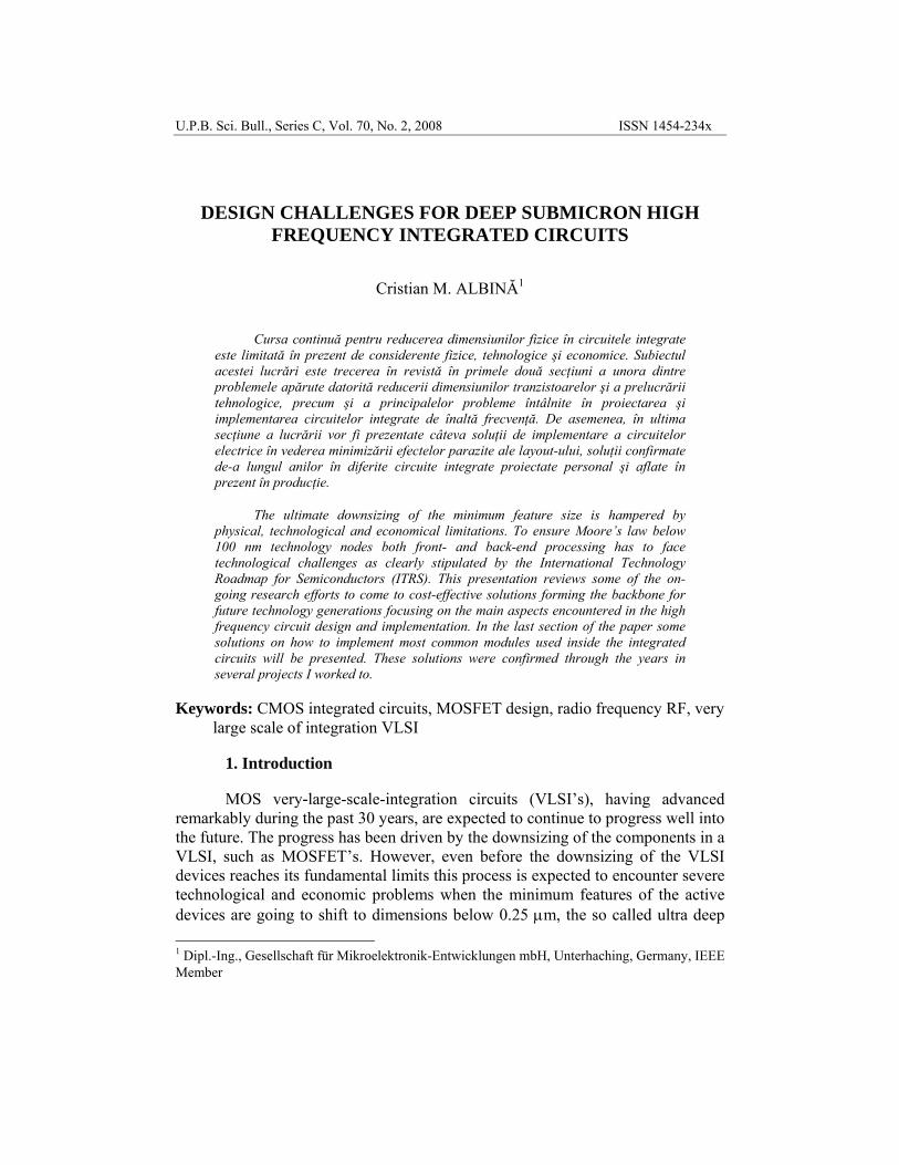
Thus, the functionality, switching and operation speed of the VLSI’s circuit is improved. Indeed, these continuous technological improvements are correctly predictable according the Moore’s law [1] [2]. Moreover, at the research level, more than several institutions have already reported successful fabrication of sub-0.1μm MOSFET devices operating at room temperature. According to ITRS for most aggressively scaled DRAM, the integration scale will reach 720 Millions of transistors by the year 2012 [3]. Additional scaling parameters are presented in Fig. 1.
Fig. 1. Trends of the MOSFET scaling in advanced VLSI technologies
There seems to be no physical limitations for feature size down to 25nm.
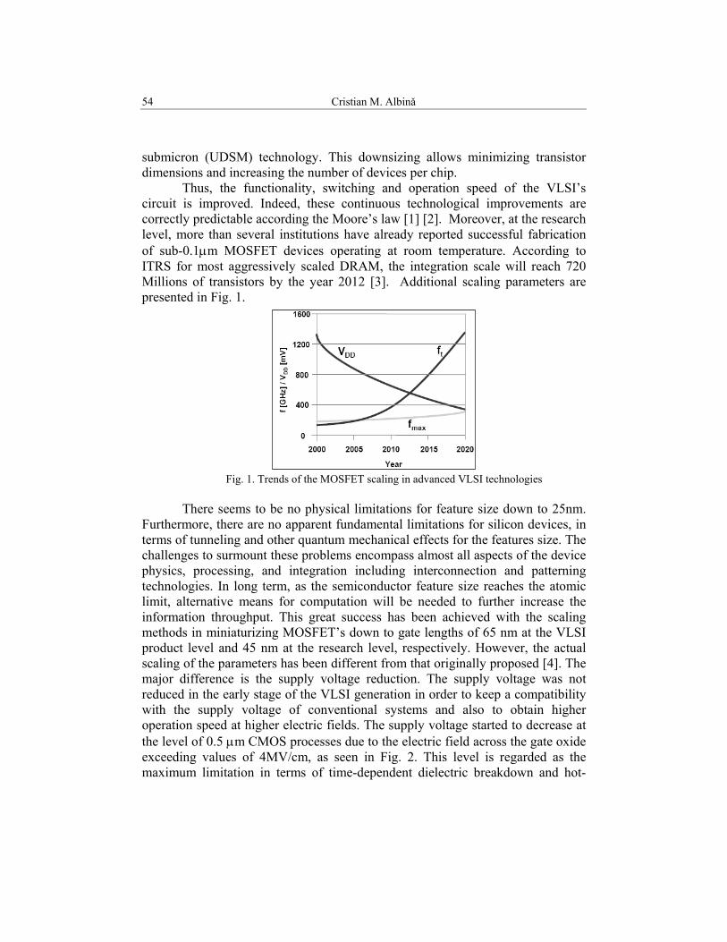
Furthermore, there are no apparent fundamental limitations for silicon devices, in terms of tunneling and other quantum mechanical effects for the features size. The challenges to surmount these problems encompass almost all aspects of the device physics, processing, and integration including interconnection and patterning technologies. In long term, as the semiconductor feature size reaches the atomic limit, alternative means for computation will be needed to further increase the information throughput. This great success has been achieved with the scaling methods in miniaturizing MOSFET’s down to gate lengths of 65 nm at the VLSI product level and 45 nm at the research level, respectively. However, the actual scaling of the parameters has been different from that originally proposed [4]. The major difference is the supply voltage reduction. The supply voltage was not reduced in the early stage of the VLSI generation in order to keep a compatibility with the supply voltage of conventional systems and also to obtain higher operation speed at higher electric fields. The supply voltage started to decrease at the level of 0.5 μm CMOS processes due to the electric field across the gate oxide exceeding values of 4MV/cm, as seen in Fig. 2. This level is regarded as the maximum limitation in terms of time-dependent dielectric breakdown and hot-
Design challenges for deep submicron high frequency integrated circuits
55
carrier induced degeneration for short channel transistors, generally speaking reliability issues of the MOSFET devices.
Fig. 2. Power Supply voltage projections for CMOS Technologies Now, however, it is not easy to reduce supply voltage because of
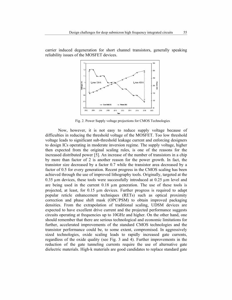
difficulties in reducing the threshold voltage of the MOSFET. Too low threshold voltage leads to significant sub-threshold leakage current and enforcing designers to design ICs operating in moderate inversion regime. The supply voltage, higher then expected from the original scaling rules, is one of the reasons for the increased distributed power [5]. An increase of the number of transistors in a chip by more than factor of 2 is another reason for the power growth. In fact, the transistor size decreased by a factor 0.7 while the transistor area decreased by a factor of 0.5 for every generation. Recent progress in the CMOS scaling has been achieved through the use of improved lithography tools. Originally, targeted at the 0.35 μm devices, these tools were successfully introduced at 0.25 μm level and are being used in the current 0.18 μm generation. The use of these tools is projected, at least, for 0.15 μm devices. Further progress is required to adapt popular reticle enhancement techniques (RETs) such as optical proximity correction and phase shift mask (OPC/PSM) to obtain improved packaging densities. From the extrapolation of traditional scaling, UDSM devices are expected to have excellent drive current and the projected performance suggests circuits operating at frequencies up to 10GHz and higher. On the other hand, one should remember that there are serious technological and economic limitations for further, accelerated improvements of the standard CMOS technologies and the transistor performance could be, to some extent, compromised. In aggressively sized technologies, oxide scaling leads to rapidly increased gate currents, regardless of the oxide quality (see Fig. 3 and 4). Further improvements in the reduction of the gate tunneling currents require the use of alternative gate dielectric materials. High-k materials are good candidates to replace standard gate
Cristian M. Albinǎ
56
oxides. Similarly, potential solutions (e.g. low energy implantation) for advanced source/drain extension engineering, which would approach the physical limit of ultra-shallow but low-resistance junctions, have been discussed in the literature.
Fig. 3.Device gate current contributions Fig. 4 Device off-current contributions
ISrc = Source current (T, S/D) IGate = Gate leakage current direct tunneling (VDD, GOX) IGIDL = Gate induced drain leakage (VDD, GOX, S/D) IJct = Junction leakage (VDD, S/D, T)
2. Submicron technology and layout dependent effects
All the above presented effects like gate direct tunneling current, drain induced voltage threshold shift, output resistance and base width modulation, were not previously modeled [6] in versions like BSIM3v3 making necessary the introduction of new standard compact models like BSIM4 to improve the circuit simulation. Additional device physical effects related to technology are:
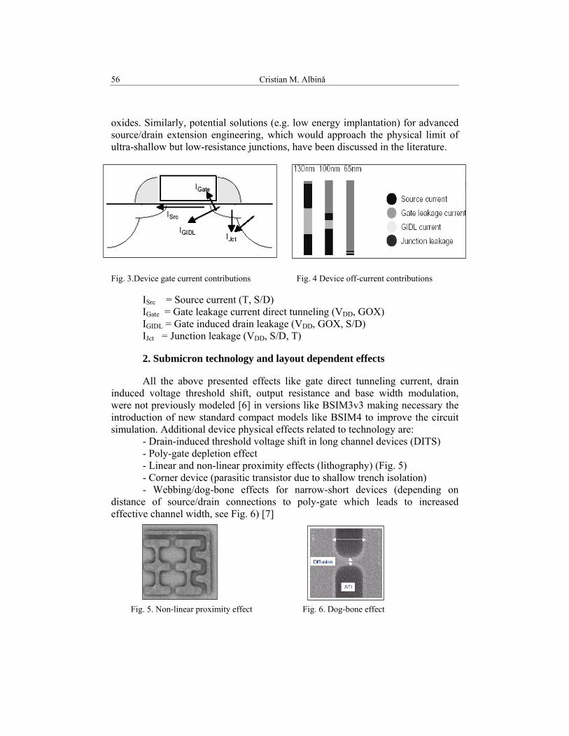
- Drain-induced threshold voltage shift in long channel devices (DITS) - Poly-gate depletion effect - Linear and non-linear proximity effects (lithography) (Fig. 5) - Corner device (parasitic transistor due to shallow trench isolation) - Webbing/dog-bone effects for narrow-short devices (depending on
distance of source/drain connections to poly-gate which leads to increased effective channel width, see Fig. 6) [7]
Fig. 5. Non-linear proximity effect Fig. 6. Dog-bone effect
Design challenges for deep submicron high frequency integrated circuits
57
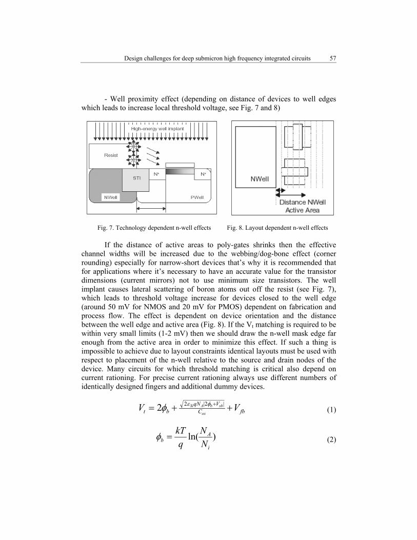
- Well proximity effect (depending on distance of devices to well edges
which leads to increase local threshold voltage, see Fig. 7 and 8)
Fig. 7. Technology dependent n-well effects Fig. 8. Layout dependent n-well effects
If the distance of active areas to poly-gates shrinks then the effective channel widths will be increased due to the webbing/dog-bone effect (corner rounding) especially for narrow-short devices that’s why it is recommended that for applications where it’s necessary to have an accurate value for the transistor dimensions (current mirrors) not to use minimum size transistors. The well implant causes lateral scattering of boron atoms out off the resist (see Fig. 7), which leads to threshold voltage increase for devices closed to the well edge (around 50 mV for NMOS and 20 mV for PMOS) dependent on fabrication and process flow. The effect is dependent on device orientation and the distance between the well edge and active area (Fig. 8). If the Vt matching is required to be within very small limits (1-2 mV) then we should draw the n-well mask edge far enough from the active area in order to minimize this effect. If such a thing is impossible to achieve due to layout constraints identical layouts must be used with respect to placement of the n-well relative to the source and drain nodes of the device. Many circuits for which threshold matching is critical also depend on current rationing. For precise current rationing always use different numbers of identically designed fingers and additional dummy devices.
fbCVqN
bt VVox
sbbASi ++= + |2|22 φεφ (1)
)ln(i
Ab N
Nq
kT=φ (2)
Cristian M. Albinǎ
58
ox
fcmsfb C
QV −= φ (3)
Sigatems φφφ −= (4) The first two components are the so called ideal threshold voltage and the
third component is the flat band voltage. Φb is the bulk potential, NA is the density of the carriers in the open semiconductor substrate. Ni is the carrier concentration of intrinsic (undoped) silicon (typically 1.45x1010cm-3 for 300 degrees K), k is the Boltzman’s constant, T the temperature and q the electronic charge. A typical value for the
qkT factor is 25.8 mV at 300 degrees K. The MOS transistor
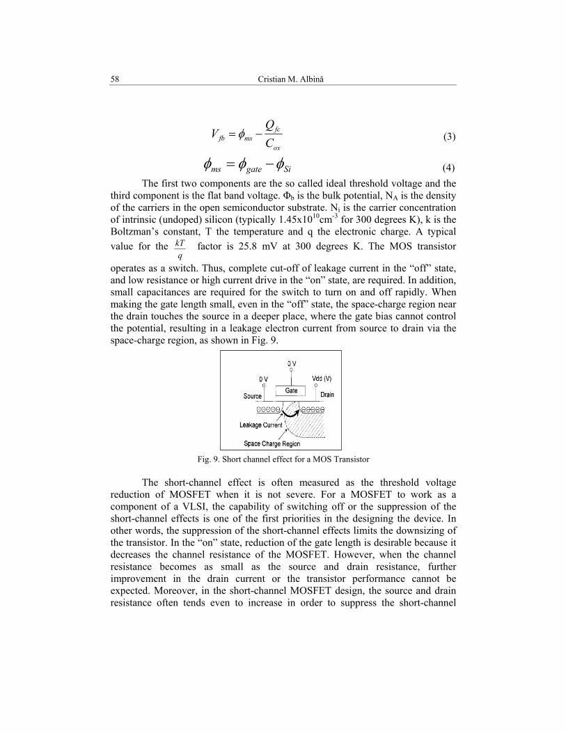
operates as a switch. Thus, complete cut-off of leakage current in the “off” state, and low resistance or high current drive in the “on” state, are required. In addition, small capacitances are required for the switch to turn on and off rapidly. When making the gate length small, even in the “off” state, the space-charge region near the drain touches the source in a deeper place, where the gate bias cannot control the potential, resulting in a leakage electron current from source to drain via the space-charge region, as shown in Fig. 9.
Fig. 9. Short channel effect for a MOS Transistor The short-channel effect is often measured as the threshold voltage
reduction of MOSFET when it is not severe. For a MOSFET to work as a component of a VLSI, the capability of switching off or the suppression of the short-channel effects is one of the first priorities in the designing the device. In other words, the suppression of the short-channel effects limits the downsizing of the transistor. In the “on” state, reduction of the gate length is desirable because it decreases the channel resistance of the MOSFET. However, when the channel resistance becomes as small as the source and drain resistance, further improvement in the drain current or the transistor performance cannot be expected. Moreover, in the short-channel MOSFET design, the source and drain resistance often tends even to increase in order to suppress the short-channel
Design challenges for deep submicron high frequency integrated circuits
59
effects. Thus, it is important to consider ways for reducing the total resistance while keeping the suppression of the short-channel effects. The capacitances of the MOSFET usually decrease with the downsizing, but care should be taken when the fringing portion is dominant or when impurity concentration of the substrate is large in the short-channel transistor design. Thus, for the MOSFET downsizing, the suppression of the short-channel effects with the improvement of the total resistance and capacitances are required.
3. RF CMOS Transistor downsizing limitations
The need for miniaturization, low power consumption, low cost and the advance towards higher frequencies for wireless and applications are critical trends influencing the direction of communications system development. Unrestricted access to information, anywhere, any place, and any time, will be characteristic for state-of-the-art information systems of the 21st century. The current cycle sees radio frequency (RF) and microwave integrated circuit engineering having grown rapidly in importance in recent years, stimulated, in particular, by booming digital mobile communications. Although the use of standard CMOS has a number of advantages, including integration capabilities and operation from low supply voltages, it has the reputation of not being appropriate for high bit rates. Recently, however, CMOS has been demonstrated to be a viable technology for high bit rate broadband circuit design at 10 Gbit/s. With gate lengths of 180 nm and below, MOS transistors offer impressive performance in terms of cut-off frequency fT and maximum oscillation frequency fmax. Combined with innovative circuit design this enables the use of CMOS technology in multi-gigabit/s applications. Another important issue in high-speed CMOS design is parasitic capacitance of devices and interconnects. The large number of copper interconnect layers available in modern CMOS processes facilitates the integration of on-chip spiral inductors which are required for inductive peaking. For RF designs, the most critical device parameters are the transconductance coefficient μCox and the parasitic capacitances, µ is the carriers’ mobility and Cox is the oxide capacitance.
ox
oxox t
C ε= (5)
Coxeffeff
m ECW
g2μ
= for VDS > VDSAT (6)
Based on this coefficient, we can calculate the transconductance of a
transistor gm and we see that is limited at the upper side by velocity saturation. In
Cristian M. Albinǎ
60
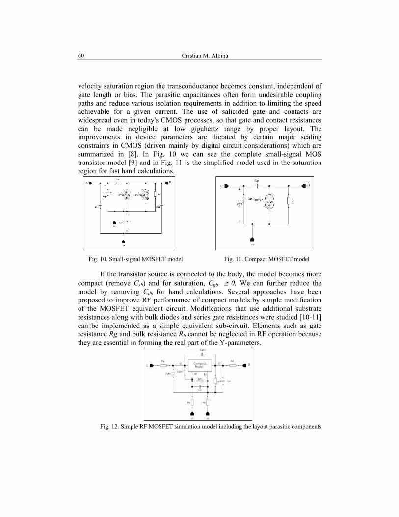
velocity saturation region the transconductance becomes constant, independent of gate length or bias. The parasitic capacitances often form undesirable coupling paths and reduce various isolation requirements in addition to limiting the speed achievable for a given current. The use of salicided gate and contacts are widespread even in today's CMOS processes, so that gate and contact resistances can be made negligible at low gigahertz range by proper layout. The improvements in device parameters are dictated by certain major scaling constraints in CMOS (driven mainly by digital circuit considerations) which are summarized in [8]. In Fig. 10 we can see the complete small-signal MOS transistor model [9] and in Fig. 11 is the simplified model used in the saturation region for fast hand calculations.
Fig. 10. Small-signal MOSFET model Fig. 11. Compact MOSFET model
If the transistor source is connected to the body, the model becomes more
compact (remove Csb) and for saturation, Cgb ≅ 0. We can further reduce the model by removing Cdb for hand calculations. Several approaches have been proposed to improve RF performance of compact models by simple modification of the MOSFET equivalent circuit. Modifications that use additional substrate resistances along with bulk diodes and series gate resistances were studied [10-11] can be implemented as a simple equivalent sub-circuit. Elements such as gate resistance Rg and bulk resistance Rb cannot be neglected in RF operation because they are essential in forming the real part of the Y-parameters.
Fig. 12. Simple RF MOSFET simulation model including the layout parasitic components
Design challenges for deep submicron high frequency integrated circuits
61
WLL
Wn
RR con
f
shg
ρ+
××= 234
(7)
Rsh is the sheet resistivity and nf is the number of fingers. In some simulators, Rg and Rb are already parts of the MOSFET model, so that a sub-circuit definition specific to RF is not needed (Fig. 12). All the terminal resistances, as well as the substrate resistances are bias dependent. The bias dependence of the source and drain resistances are mostly due to the lightly doped drain (LDD) regions, where ion implantation is used in the submicron technologies for the reduction of the high electric potential drops in the drain region and to compensate the hot electron effects that leads to the degeneration of the gate oxide and reduces the device reliability. The primary objective is to decrease both the minimum channel length and gate-oxide thickness, in order to improve the achievable transconductance and increase integration density. Reduction of oxide thickness, however, lowers the threshold voltage, which must be compensated by increasing channel and, consequently, drain and source diffusion doping concentrations. From 1 μm to 0.25 μm CMOS, the doping concentration, in the last decade, has increased by an order of magnitude. It is clear that junction capacitances increase rapidly as process scales down, while the overlap capacitance stays roughly constant, due to reduction of the gate-drain overlap. Also worth mentioning is that although the minimum feature size Lmin has improved by a factor of 3, the design rules for minimum drain and source width have decreased by only 1.5 times. This means the capacitance per μm of gate width due to CJ remains roughly constant as the technology scales. Since the gate oxide thickness scales by the same ratio as Lmin, gate capacitance per μm of gate-width also remains constant. Thus depending on the capacitance that is involved, the capacitive load per μm gate-width either remains constant or increases. The benefit of improved performance therefore only comes from increased transconductance.
4. RF basic blocks layout implementation
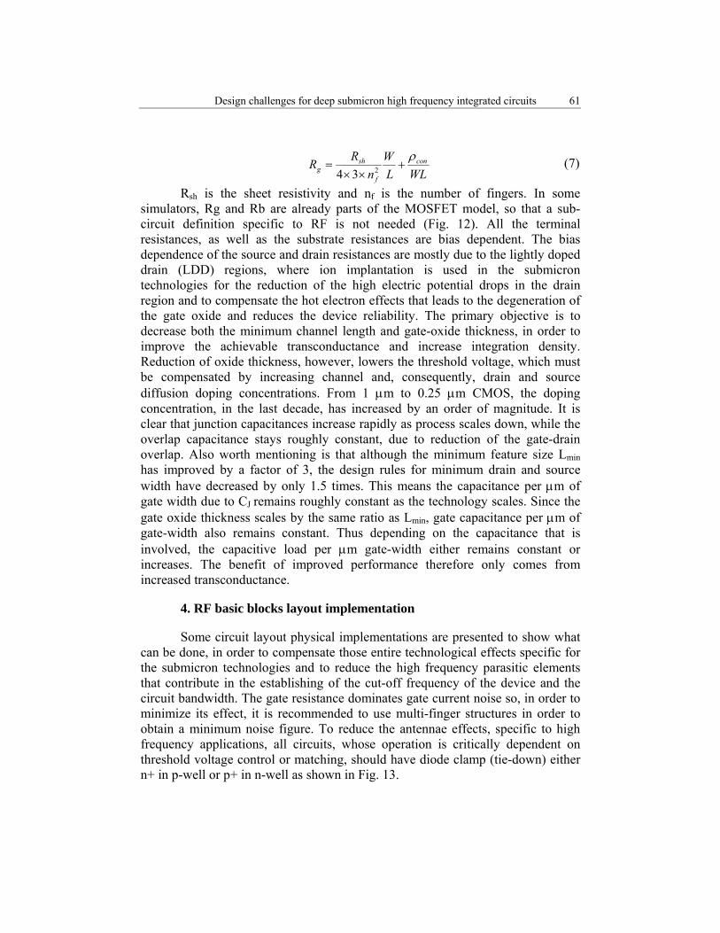
Some circuit layout physical implementations are presented to show what can be done, in order to compensate those entire technological effects specific for the submicron technologies and to reduce the high frequency parasitic elements that contribute in the establishing of the cut-off frequency of the device and the circuit bandwidth. The gate resistance dominates gate current noise so, in order to minimize its effect, it is recommended to use multi-finger structures in order to obtain a minimum noise figure. To reduce the antennae effects, specific to high frequency applications, all circuits, whose operation is critically dependent on threshold voltage control or matching, should have diode clamp (tie-down) either n+ in p-well or p+ in n-well as shown in Fig. 13.
Cristian M. Albinǎ
62
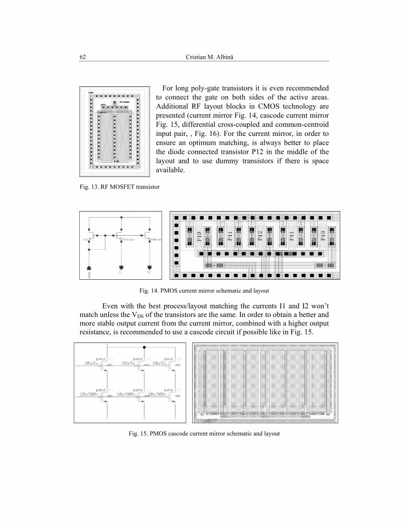
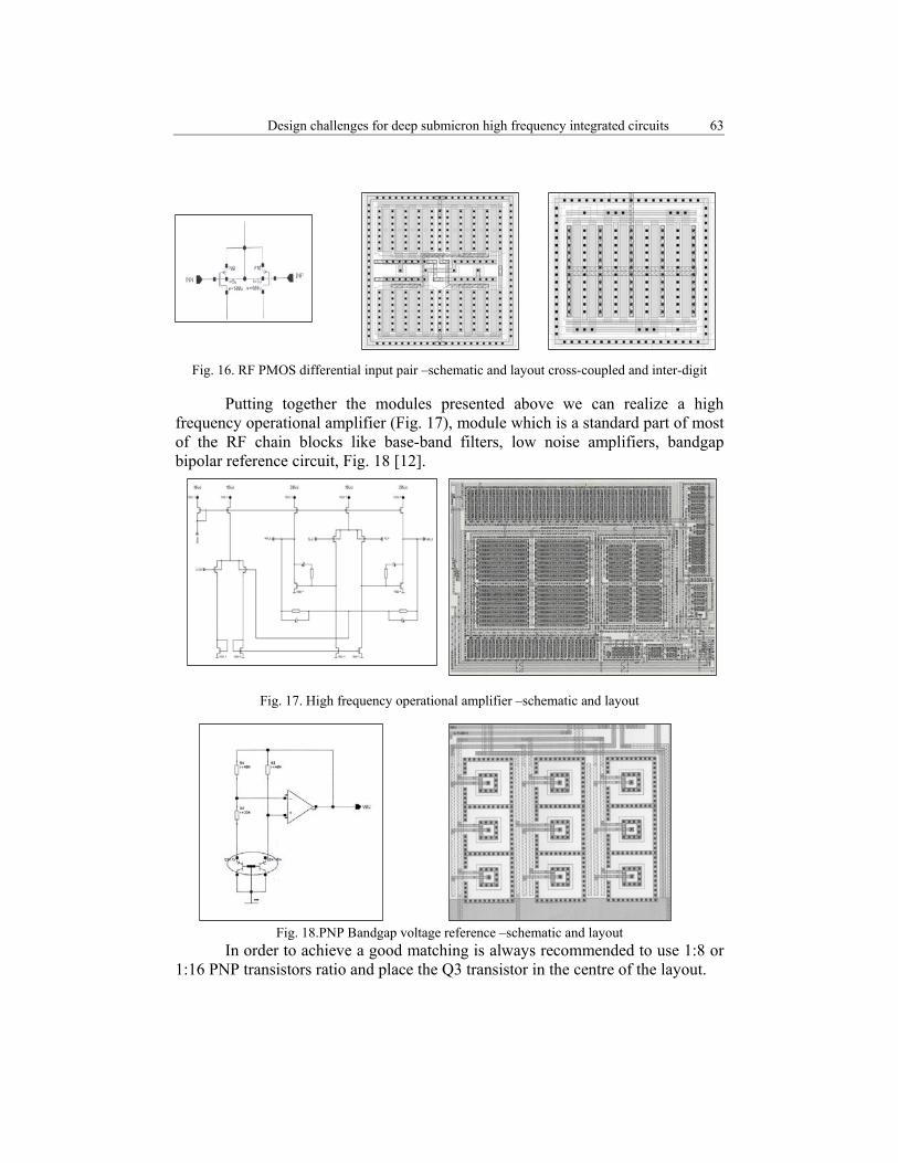
For long poly-gate transistors it is even recommended to connect the gate on both sides of the active areas. Additional RF layout blocks in CMOS technology are presented (current mirror Fig. 14, cascode current mirror Fig. 15, differential cross-coupled and common-centroid input pair, , Fig. 16). For the current mirror, in order to ensure an optimum matching, is always better to place the diode connected transistor P12 in the middle of the layout and to use dummy transistors if there is space available.
Fig. 13. RF MOSFET transistor
Fig. 14. PMOS current mirror schematic and layout
Even with the best process/layout matching the currents I1 and I2 won’t
match unless the VDS of the transistors are the same. In order to obtain a better and more stable output current from the current mirror, combined with a higher output resistance, is recommended to use a cascode circuit if possible like in Fig. 15.
Fig. 15. PMOS cascode current mirror schematic and layout
Design challenges for deep submicron high frequency integrated circuits
63
Fig. 16. RF PMOS differential input pair –schematic and layout cross-coupled and inter-digit
Putting together the modules presented above we can realize a high frequency operational amplifier (Fig. 17), module which is a standard part of most of the RF chain blocks like base-band filters, low noise amplifiers, bandgap bipolar reference circuit, Fig. 18 [12].
Fig. 17. High frequency operational amplifier –schematic and layout
Fig. 18.PNP Bandgap voltage reference –schematic and layout In order to achieve a good matching is always recommended to use 1:8 or
1:16 PNP transistors ratio and place the Q3 transistor in the centre of the layout.
Cristian M. Albinǎ
64
5. Conclusions
The trend towards deep sub-micron technologies has resulted in the exploration by several research groups of the possible use of CMOS technologies for the design of RF circuits. Especially the development of new receiver topologies, such as wide-band-IF and low-IF topologies, in combination with highly linear down-converters, has opened the way to fully integrated down-converters with no external filters or components. However, due to the moderate speed performance of the present sub-micron technologies, lower noise circuits in combination with less power drain have to be worked out. High performance low phase noise, low power drain, fully integrated VCO circuits have been demonstrated in CMOS. Today, even low phase noise performances with optimized integrated spiral inductors in standard CMOS technologies without any post-processing, tuning, trimming or external components have been realized. This opens the way towards fully integrated receiver circuits. Again, thanks to the trends towards deep sub-micron technologies fully integrated CMOS transmitter circuits with acceptable power consumption will hopefully be feasible.
R E F E R E N C E S
[1] Moore, G.E, “Cramming more components onto integrated circuits”, Proceedings of the IEEE 2001, Vol.86, pp. 82-85 (Reprinted from Electronics, April19, 1965, pp. 114-117).
[2] Ulaby, F.T, “The Legacy of Moore’s Law”, Proceedings of the IEEE 2006, Volume 94, pp. 1251-1252.
[3] International Technology Roadmap for Semiconductors, 2005 Edition, http://www.itrs.net/ Links/2005ITRS/Home2005.html.
[4] Bohr, M., “A 30 Year Retrospective on Dennard’s MOSFET Scaling Paper”, IEEE Newsletter Winter 2007, Vol.12, No. 1, pp. 11-13.
[5] Constantinescu, C., “Trends and Challenges in VLSI circuit reliability”, Micro IEEE Newsletter July-August 2003, Vol.23, Issue 4, pp. 14-19.
[6] Rusu, A., “Conducţie Electrică Neliniară în Structuri Semiconductoare”, Editura Academiei Române, Bucureşti, 2000, Capitolul 8 Tranzistorul MOS Model fizic general, pp. 212-213.
[7] Flautner, K., “Simple techniques for reducing leakage power,” Ann. Int’l. Symposium for Computer Architecture, ISCA29, IEEE CS Press 2002, pp. 148-157.
[8] Allstot, D.J., Choi, K., “Parasitic aware design and optimization of a CMOS RF circuit”, Circuits and Systems I: Regular Papers, IEEE Transactions on, Vol. 52, Dec. 2005, pp.3223-3232.
[9] Rusu, A., “Modelarea componentelor microelectronice active”, Editura Academiei Române, Bucureşti, 1990, Capitolul 4 Modelarea Tranzistoarelor MOS, pp.50-84.
[10] Razavi, B., “CMOS Receiver Front End” IEEE Journal of Solid State Circuits, Jan. 2006, pp.17-22.
[11] Elgamel, M.A., Bayoumi, M.A., “Noise analysis and optimization in deep submicron technology” IEEE Circuits and Systems Magazine, 2003, pp.6-17.
[12] Manolescu, A., “Analog Integrated Circuits” Chapter 3 Building blocks of Analog Integrated Circuits, Editura FOTON Internaţional, Bucureşti, 1999, pp.109-112.