CALCULATOARE NUMERICE -...
36
Universitatea POLITEHNICA din Bucureşti Facultatea de Automatică şi Calculatoare Catedra de Calculatoare http://www.csit-sun.pub.ro CALCULATOARE NUMERICE Proiect de semestru – anul III Prof. Îndrumător: As. Dr. Ing. Decebal Popescu Studenţi:Carauş Serghei, Bogdan Alexandru , Duţă Laura,Gartner Alexandru,Herişanu Alexandru Adresă de contact: [email protected] Bucureşti 2003 Pg.1/36
Transcript of CALCULATOARE NUMERICE -...
Universitatea POLITEHNICA din BucureştiFacultatea de Automatică şi Calculatoare
Catedra de Calculatoarehttp://www.csit-sun.pub.ro
CALCULATOARE NUMERICE
Proiect de semestru – anul III
Prof. Îndrumător:As. Dr. Ing. Decebal Popescu
Studenţi:Carauş Serghei, Bogdan Alexandru ,Duţă Laura,Gartner Alexandru,Herişanu Alexandru
Adresă de contact: [email protected]
Bucureşti 2003
Pg.1/36
Project subject: VERILOG MICROPROCESSOR
Abstract
The project is designed to extend the capabilities of the GNOMEmicroprocessor, using DWARF. There are also descriptions and pictures ofthe internal structure of the microprocessor, the way modules areinterconnected one with each other and also the main differences betweenthe microprocessor in GNOME and the one in DWARF. The main functionsand architecture of the microprocessor have been explained here, also thereare some tables containing the DWARF’s instruction set encoding, and theDWARF’s instruction set. This project contains programs for each moduledesigned in Verilog, it contains examples of simulations and outputs.
Abstract
Acest proiect are ca scop extinderea capabilitatilor microprocesoruluiGNOME, utilizand DWARF. Sunt prezentate de asemenea si descrieri siimagini ale structurii intrene a microprocesorului, modul in care suntinterconectate modulele intre ele si principalele diferente dintremicropocesorul realizat in GNOME si cel in DWARF. Sunt explicateprincipalele functii si arhitectura microprocesorului si sunt prezentate si setulde instructiuni codificate alaturi de setul de instructiuni al microprocesorului.Acest proiect contine programe proiectate in Verilog pentru fiecare modul,contine exemple de simulari si fisiere cu rezultate.
Pg.2/36
Table of Contents
Abstract......................................................................................................................2Abstract......................................................................................................................2Part I.......................................................................................................................... 6
Introduction...........................................................................................................68-bit Datapath...................................................................................................6Register Set...................................................................................................... 6Indexed and Indirect Addressing...................................................................... 7Input and Output Ports.....................................................................................7Subroutine Call and Return Instructions...........................................................8Interrupt Handling............................................................................................ 8
DWARF instruction set......................................................................................... 9DWARF Basic Architecture................................................................................13
Stack Pointer (SP).......................................................................................... 14Register set(R0-R7)........................................................................................14I/O port(IOP) .................................................................................................14Address selector............................................................................................. 14Interrupt detector............................................................................................15D bus.............................................................................................................. 15DWARF’s Register Set and ALU...................................................................15DWARF’s Arithmetic Circuitry......................................................................16DWARF’s carry flag.......................................................................................16DWARF’s Program Counter, Stack Pointer, Address Selector, and RAMControl Circuitry............................................................................................ 17Detailed Circuitry for DWARF’s Address Multiplexer.................................. 18DWARF’s I/O Port Circuitry......................................................................... 19DWARF’s Interrupt-Handling Circuitry.........................................................20Data Bus Interface to the External RAM....................................................... 22DWARF Instruction Decoder.........................................................................22
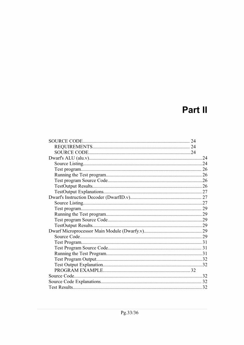
Part II....................................................................................................................... 25Source Code........................................................................................................25
Requirements.................................................................................................. 25Source Code................................................................................................... 25
Dwarf's ALU (alu.v).................................................................................. 25Source Listing....................................................................................... 25Test program.........................................................................................27Running the Test program.....................................................................27Test program Source Code................................................................... 27TestOutput Results................................................................................27TestOutput Explanations.......................................................................28
Dwarf's Instruction Decoder (DwarfID.v).................................................28Source Listing....................................................................................... 28
Pg.3/36
Test program.........................................................................................30Running the Test program.....................................................................30Test program Source Code................................................................... 30TestOutput Results................................................................................30
Dwarf Microprocessor Main Module (Dwarfy.v)......................................30Source Code..........................................................................................30Test Program.........................................................................................32Test Program Source Code...................................................................32Running the Test Program.................................................................... 32Test Program Output............................................................................ 33Test Output Explanation....................................................................... 33
Program Example........................................................................................... 33APPENDIX..............................................................................................................35
CHANGELOG....................................................................................................35TODO................................................................................................................. 35Instructions Set....................................................................................................36Bibliography........................................................................................................ 37
Pg.4/36
Part I
INTRODUCTION.......................................................................................58-BIT DATAPATH................................................................................ 5REGISTER SET..................................................................................... 5INDEXED AND INDIRECT ADDRESSING.......................................6INPUT AND OUTPUT PORTS.............................................................6SUBROUTINE CALL AND RETURN INSTRUCTIONS................... 7INTERRUPT HANDLING.................................................................... 7
Pg.5/36
Part I
Introduction
In this project we tried to extend the capabilities of the Gnomemicroprocessor to create the Dwarf microprocessor.
This added capabilities are:• The ability to handle 8-bit data• A register set• Indexed and indirect addresssing• Input and output ports• Subroutine call and return instructions• Interrupt handling
8-bit Datapath
The datapath width can easily be increased to handle 8-bit data bz addingmore bits to the ALU and the accumulator. However, this means that immediate-mode data can no longer be stored directly in the instruction opcode because itwould consume all 8 bits. Therefor, immediate-mode data will have to be stored inthe memorz location just after the instruction opcode. Once the modification ismade, we might as well increase the data memorz to 256 bytes. With these changes,many of the instructions will consume 2 bytes and require two fetches to read fromthe external RAM. These complications will have to be accounted for in theDWARF instruction decoder.
Register Set
The GNOME operated on its accumulator using operands fetched fromexternal RAM. A microprocessor can execute more swiftly if it can get operandsfrom a set of internal registers rather than bringing them in from outside the chip.These registers can store intermediate values and provide new addressing modes. Aset of eight registers provides adequate internal storage and the register addressescan be stored in the opcode using only three of eight bits.
Pg.6/36
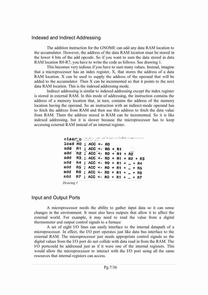
Indexed and Indirect Addressing
The addition instruction for the GNOME can add any data RAM location tothe accumulator. However, the address of the data RAM location must be stored inthe lower 4 bits of the add opcode. So if you want to sum the data stored in dataRAM location R0-R7, you have to write the code as follows. See drawing 1.
This becomes very tedious if you have to sum many values. Instead, imaginethat a microprocessor has an index register, X, that stores the address of a dataRAM location. X can be used to supply the address of the operand that will beadded to the accumulator. Then X can be incremented so that it points to the nextdata RAM location. This is the indexed addressing mode.
Indirect addressing is similar to indexed addressing except the index registeris stored in external RAM. In this mode of addressing, the instruction contains theaddress of a memory location that, in turn, contains the address of the memorylocation having the operand. So an instruction with an indirect-mode operand hasto fetch the address from RAM and then use this address to fetch the data valuefrom RAM. Them the address stored in RAM can be incremented. So it is likeindexed addressing, but it is slower because the microprocessor has to keepaccessing external RAM instead of an internal register.
Input and Output Ports
A microprocessor needs the ability to gather input data so it can sensechanges in the environment. It must also have outputs that allow it to affect theexternal world. For example, it may need to read the value from a digitalthermometer and output control signals to a furnace
A set of eight I/O lines can easily interface to the internal datapath of amicroprocessor. In effect, the I/O port operates just like data bus interface to theexternal RAM. The microprocessor just needs appropriate control signals so thedigital values from the I/O port do not collide with data read in from the RAM. TheI/O portcould be addressed just as if it were one of the internal registers. Thiswould allow the microprocessor to interact with the I/O port using all the sameresources that internal registers can access.
Pg.7/36
Drawing 1
Subroutine Call and Return Instructions
A program that performs a particular operation at several points in theprogram will be smaller if the common operation is placed in a subroutine. Anexample of a likely candidate for a subroutine is the code for doing 8-bit addition.Then whenever 8-bit addition is needed, the program can jump to the subroutineand perform the operation. After a subroutine is completed, the program returns towhere it was previously and continues. This saves the programmer from having toreplicate the code whenever the addition operation is needed.
The multiple SAVE registers form what is called a subroutine stack.Addresses are pushed on the stack whenever a jsr instruction is executed. Theseaddresses are popped off the stack and into the PC whenever a ret instruction isexecuted. Microprocessors often store their stack in external RAM and use adedicated register(called a stack pointer) to keep track of where the top of the stackis in memory.
Interrupt Handling
Subroutine calls and returns occur under the direction of the program.There are situations, however, when external conditions demand immediateattention and the flow of control must be abruptly changed. These interrupts are notevents that the microprocessor can anticipate and plan for. Instead, it must saveenough information about its current state, jump to a section of code that handlesthe interrupt(called an interrupt service routine or ISR), and then restore its stateand continue its original flow of instructions.
The state information that the microprocessor must store after an interruptis received is, at minimum, the value of the program counter. With this information,the microprocessor can return to where it was after it finishes processing theinterrupt. But the microprocessor must also save the values in registers and flags aswell if these might be altered by instructions that service the interrupt. The values ofthe PC, registers, and flags at any given time are typically called the context. Acommon technique for saving the context is to push the values onto the stack usingthe same techniques employed during subroutine calls. Then the context can berestored by popping it off the stack at the end of the ISR
Pg.8/36
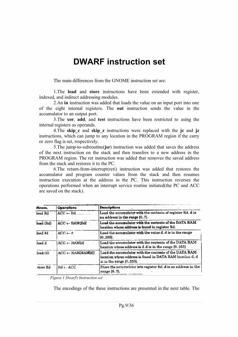
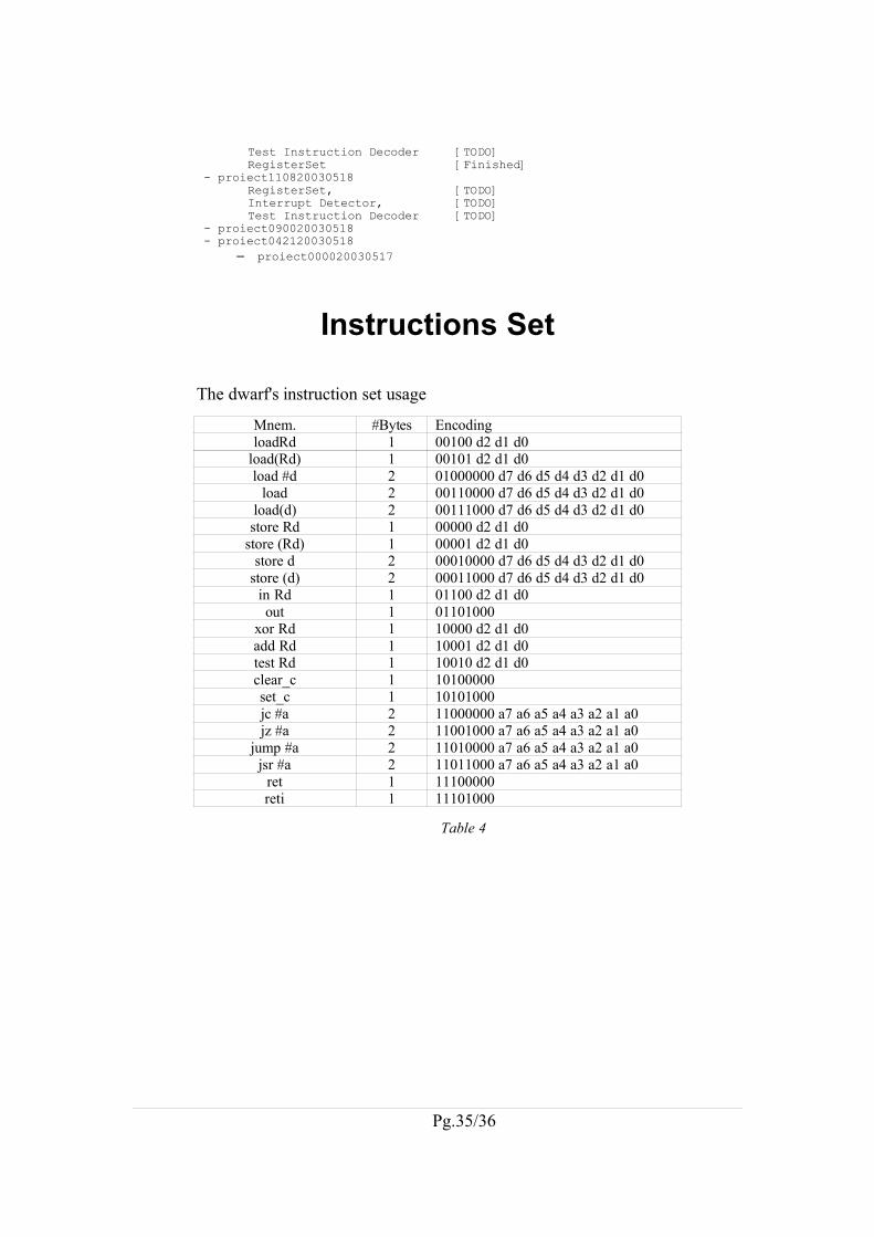
DWARF instruction set
The main differences from the GNOME instruction set are:
1.The load and store instructions have been extended with register,indexed, and indirect addressing modules.
2.An in instruction was added that loads the value on an input port into oneof the eight internal registers. The out instruction sends the value in theaccumulator to an output port.
3.The xor, add, and test instructions have been restricted to using theinternal registers as operands.
4.The skip_c and skip_z instructions were replaced with the jc and jzinstructions, which can jump to any location in the PROGRAM region if the carryor zero flag is set, respectively.
5.The jump-to-subroutine(jsr) instruction was added that saves the addressof the next instruction on the stack and then transfers to a new address in thePROGRAM region. The ret instruction was added that removes the saved addressfrom the stack and restores it to the PC.
6.The return-from-interrupt(reti) instruction was added that restores theaccumulator and program counter values from the stack and then resumesinstruction execution at the address in the PC. This instruction reverses theoperations performed when an interrupt service routine initiated(the PC and ACCare saved on the stack).
The encodings of the these instructions are presented in the next table. The
Pg.9/36
Figura 1 Dwarf's Instruction set
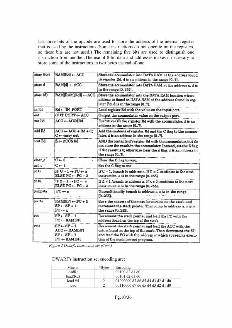
last three bits of the opcode are used to store the address of the internal registerthat is used by the instructions.(Some instructions do not operate on the registers,so these bits are not used.) The remaining five bits are used to distinguish oneinstruction from another.The use of 8-bit data and addresses makes it necessary tostore some of the instructions in two bytes instead of one.
DWARF's instruction set encoding are:
Mnem. #Bytes EncodingloadRd 1 00100 d2 d1 d0
load(Rd) 1 00101 d2 d1 d0load #d 2 01000000 d7 d6 d5 d4 d3 d2 d1 d0
load 2 00110000 d7 d6 d5 d4 d3 d2 d1 d0
Pg.10/36
Figura 2 Dwarf's Instruction set (Cont.)
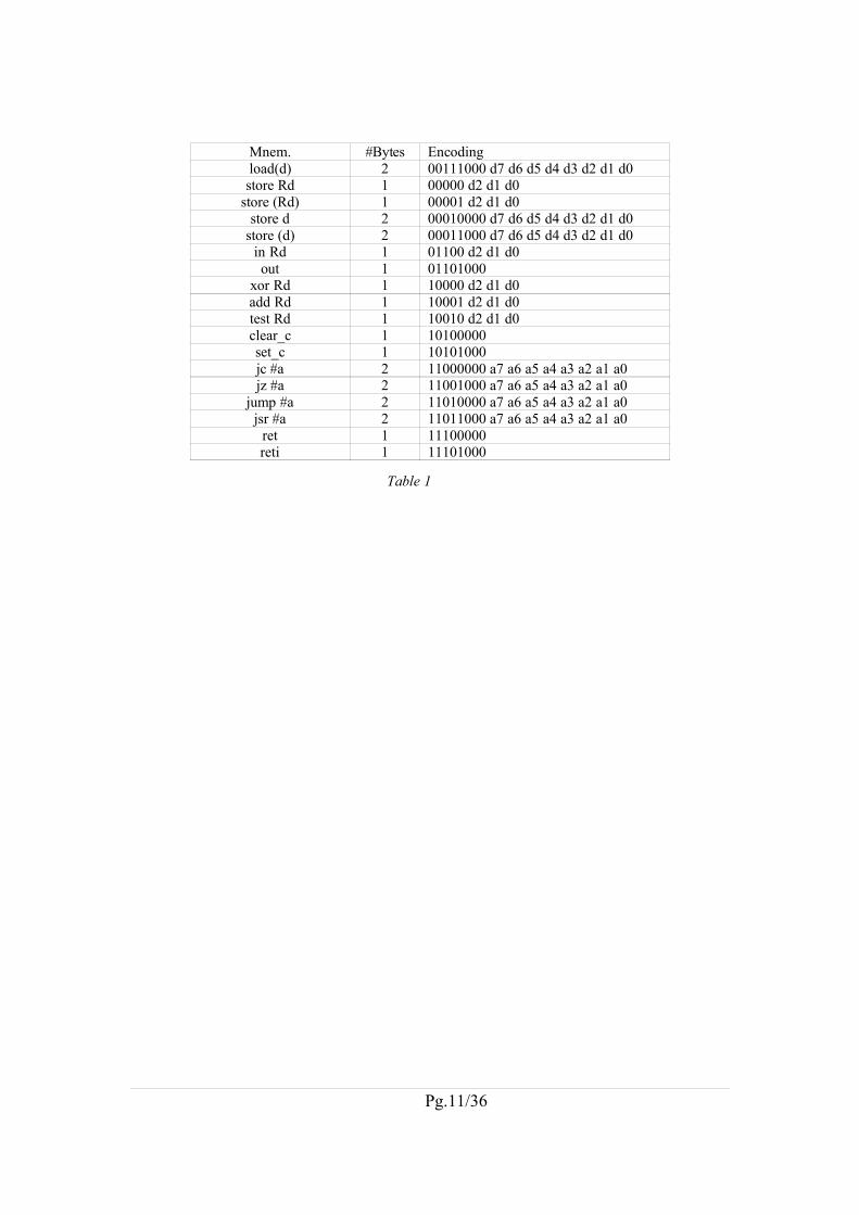
Mnem. #Bytes Encodingload(d) 2 00111000 d7 d6 d5 d4 d3 d2 d1 d0store Rd 1 00000 d2 d1 d0
store (Rd) 1 00001 d2 d1 d0store d 2 00010000 d7 d6 d5 d4 d3 d2 d1 d0
store (d) 2 00011000 d7 d6 d5 d4 d3 d2 d1 d0in Rd 1 01100 d2 d1 d0out 1 01101000
xor Rd 1 10000 d2 d1 d0add Rd 1 10001 d2 d1 d0test Rd 1 10010 d2 d1 d0clear_c 1 10100000 set_c 1 10101000 jc #a 2 11000000 a7 a6 a5 a4 a3 a2 a1 a0jz #a 2 11001000 a7 a6 a5 a4 a3 a2 a1 a0
jump #a 2 11010000 a7 a6 a5 a4 a3 a2 a1 a0jsr #a 2 11011000 a7 a6 a5 a4 a3 a2 a1 a0
ret 1 11100000reti 1 11101000
Table 1
Pg.11/36
Part I (Cont)
DWARF INSTRUCTION SET................................................................... 9
Pg.12/36
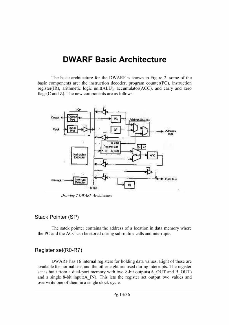
DWARF Basic Architecture
The basic architecture for the DWARF is shown in Figure 2. some of thebasic components are: the instruction decoder, program counter(PC), instructionregister(IR), arithmetic logic unit(ALU), accumulator(ACC), and carry and zeroflags(C and Z). The new components are as follows:
Stack Pointer (SP)
The satck pointer contains the address of a location in data memory wherethe PC and the ACC can be stored during subroutine calls and interrupts.
Register set(R0-R7)
DWARF has 16 internal registers for holding data values. Eight of these areavailable for normal use, and the other eight are used during interrupts. The registerset is built from a dual-port memory with two 8-bit outputs(A_OUT and B_OUT)and a single 8-bit input(A_IN). This lets the register set output two values andoverwrite one of them in a single clock cycle.
Pg.13/36
Drawing 2 DWARF Architecture
I/O port(IOP)
DWARF has eight output pins and eight input pins dedicated to general-purpose input/output.
Address selector
DWARF divides the external memory into three regions: PROGRAM(256bytes), DATA(256 bytes), and STACK(256 bytes). The address selector enablesone of these regions and sends it an address from one of three sources: ThePROGRAM region is addressed by the PC; the STACK region is addressed by theSP; and the DATA region is addressed by the value held in one of the registers.
Interrupt detector
A rising edge on the interrupt pin (INT) triggers the interrupt circuitry,which alerts DWARF of the need to alter its sequence of instructions.
D bus
This bus ties most of the other components together. It can be driven by thePC, the B output of the register set, the ACC, the input side of the IOP, and theexternal data bus that connects to the external RAM. In turn, the value on the D-bus can be loaded into the PC, the A_IN input of the register set, the ACC, theoutput side of the IOP, and the external RAM.
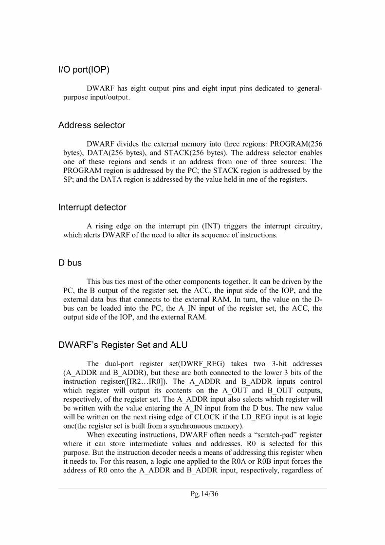
DWARF’s Register Set and ALU
The dual-port register set(DWRF_REG) takes two 3-bit addresses(A_ADDR and B_ADDR), but these are both connected to the lower 3 bits of theinstruction register([IR2…IR0]). The A_ADDR and B_ADDR inputs controlwhich register will output its contents on the A_OUT and B_OUT outputs,respectively, of the register set. The A_ADDR input also selects which register willbe written with the value entering the A_IN input from the D bus. The new valuewill be written on the next rising edge of CLOCK if the LD_REG input is at logicone(the register set is built from a synchronuous memory).
When executing instructions, DWARF often needs a “scratch-pad” registerwhere it can store intermediate values and addresses. R0 is selected for thispurpose. But the instruction decoder needs a means of addressing this register whenit needs to. For this reason, a logic one applied to the R0A or R0B input forces theaddress of R0 onto the A_ADDR and B_ADDR input, respectively, regardless of
Pg.14/36
the register address stored in the instruction register.
The register set actually contains 16 registers, so the BANK_SEL inputselects one of two banks of eight registers. The IFLAG signal is high during theexecution of an interrupt service routine, and this is used to switch the registerbanks. This gives the interrupt service routine its own set of registers to use andprevents it from altering the values in the registers used during DWARF’s normaloperations
The value on B_OUT output of the register set can be driven onto the Dbus by raising the DRV_D_REG signal. This enables the drivers of the internaltristate buffer(BUFES) so the register value can pass through. This operation isneeded when a value from the register set is being transferred to another section ofDWARF’s circuitry or into external RAM.
The details of the DWARF register set are shown in Figure 4. The heart ofthe register set is a dual-port synchronous RAM(RAM16X8D) from the standardpart list. The BANK_SEL input drives the most-significant bit of both registeraddresses. Two sets of AND gates are provided to force the register addresses tozero(the address of R0) under the control of the R0A and R0B inputs.
The ALU (Figure 3) contains the circuitry for adding and XORing valuesand for storing the accumulator and carry and status flags. The 8-bit operands enterthe ALU through the [R7…R0] inputs from the register set’s A_OUT output andthrough the [A7…A0] inputs from the D bus. The ADD and PASS inputs controlthe arithmetic operation performed on these operands as follows:
Pg.15/36
Drawing 3 DWARF’s register set and ALU
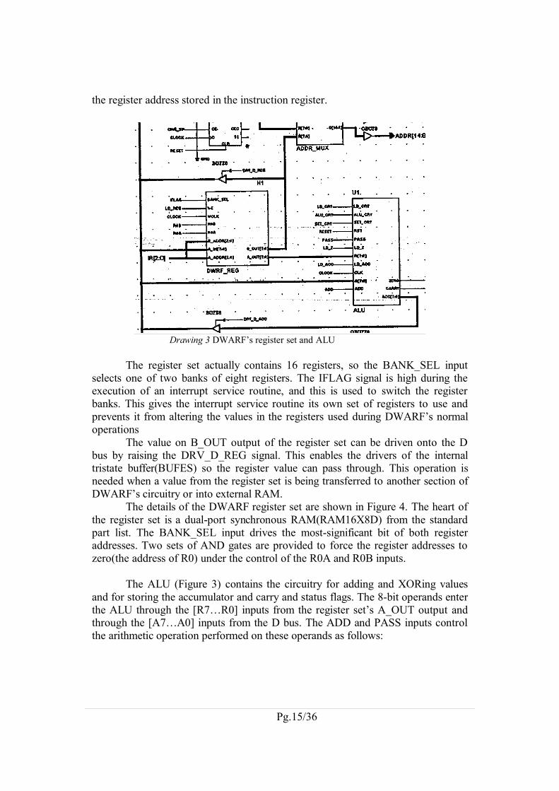
DWARF’s Arithmetic Circuitry
The details of the arithmetic circuitry are shown in Figure 5. The PASS andADD inputs control a pair of byte-wide multiplexers(identifiers H2 and H5). Themultiplexers selecteither the [A7…A0] input, the output of an 8-bit adder(ADD8),or the output of a module that does a bitewise XOR on two 8-bit values(XOR_8X8). The accumulator(module ACCUM0) is loaded with the output fromthe H2 multiplexer when LD_ACC is a logic one and there is a rising edge onCLOCK input.
DWARF’s carry flag
The zero and the carry flags are also updated when is a rising edge onCLOCK and LD_Z or LD_CRY are at logic one, respectively. The zero flag isalways loaded with the NOR of all the bits that result from a bitwise AND of the 8-bit values from the D bus and the register set.
The carry flag(Figure 7) is loaded with the carry output from the 8-bit adder(CO of the ADD8 module) if the ALU_CRY input is high. This permits thepropagation of carry bits in multibyte arithmetic operations. But if ALU_CRY=0,the carry flag is loaded with the value on the SET_CRY input, thus allowing thecarry flag to be forced to one or zero.
A logic one on the RESET input clears the accumulator and the status flagsto zero.
The carry and the zero flag exit the ALU module through the CARRY and
Pg.16/36
Drawing 4 DWARF’s ZEROTEST module
ZERO outputs. The accumulator value appears on the [ACC7…ACC0] outputs.Setting DRV_D_ACC=1 lets the accumulator drive the D bus(Figure 3). Thisprovides a path for storing the accumulator into external memory, the register set,or for feeding the accumulator back into the ALU as an operand.
DWARF’s Program Counter, Stack Pointer, Address Selector, andRAM Control Circuitry
The program counter shows that the PC(with reference identifier of PC0) isjust an 8-bit, loadable counter from the standard part list(CB8CLE).
A logic one on theLD_PC input will load the PC with a new value from theD bus on the next rising edge of CLOCK. This operation is used for jumps withinthe program. On the other hand, a logic one on the INC_PC input will cause the PCto increment its value. This operation is needed during the normal sequentialexecution of instructions.
The value in the program counter can be driven onto the D bus by raisingthe DRV_D_PC signal. This enables the drivers of the internal tristate buffer(BUFE8) so the PC value can pass through. This operation is needed when thevalue in the PC is being stored on the stack in external RAM.
The PC is cleared by raising the RESET or CLR_PC signals. This operationis needed when DWARF first starts so that the program execution can begin ataddress 0 in the PROGRAM region. The program counter is also cleared at thebeginning of an ISR.
Looking next at the stack pointer shows that the SP(with referenceidentifier of SP0) is just an 8-bit, loadable, up/down counter from the standard partlist in the schematic editor(CC8CLED).
A logic one on the CHG_SP input will cause the stack pointer to change itsvalue on a rising edge of the CLOCK signal. If a logic one is applied on theINC_SP input, the change will be an increment. Otherwise, the value in the SP willbe decremented. The increment(decrement) operation is needed when values arebeing pushed onto(popped off) the stack.
The SP is cleared by raising the RESET signal. This operation is neededwhen DWARF starts up so that stack begins growing upward from the address 0 inthe STACK region. There is no need to randomly address the contents of the stack,so the D[7:0] input to the counter is left unconnected and the load signal(L) is tiedto a logic zero.
The B output of the register set, SP, and PC are the A,B and C inputs to theaddress multiplexer module(ADDR_MUX in Figure 8, bottom right). The addressmultiplexer selects one of its inputs as the source of the lower 8-bits of the RAMaddress and sets the upper 7 bits so that the DATA,STACK,and PROGRAMmemory regions are separated. ADDR_MUX outputs the following values giventhe settings of the SEL0 and SEL1 inputs:
The DATA region of the external RAM is accessed when SEL0=SEL1=0.The B output of the register set supplies the lower 8 bits of the address while the
Pg.17/36
upper 7 bits are set to 0x7F. Thus, the DATA region lies at the top of the RAMbetween hexadecimal addresses 0x7F00 and 0x7FFF. In a similar manner, theSTACK region(SEL0=1,SEL1=0) occupies the address range 0xtE00-0x7EFF withthe satck pointer supplying the lower eight address bits. The PROGRAM region(SEL0=SEL1=1) occupies the lowest 256 bytes of RAM(0x0000-0x00FF) with thePC, naturally, acting as the source for the lower 8 bits of address in this region.
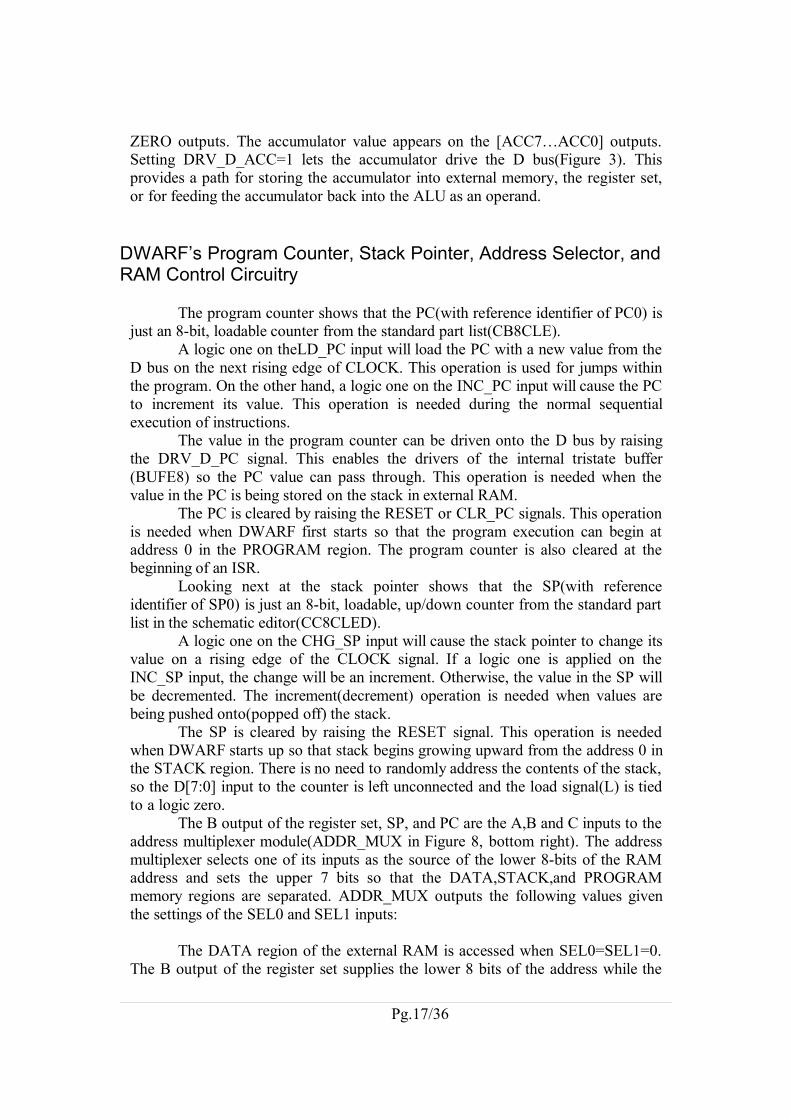
Detailed Circuitry for DWARF’s Address Multiplexer
It consists mainly of two 8-bit multiplexers that work in series to steer oneof the three byte-wide A,B, or C inputs to the [O7..O0] output under the directionof the SEL0 and SEL1 inputs. SEL0 and SEL1 also go to a set of inverters thatgenerate the correct bit pattern for each memory region on the upper 7 bits of thememory address.
Miscellaneous circuitry for driving the control inputs of the external RAM isshown in the upper right portion of Figure 8. The RAM is permanently enabled bytyping the chip select(CS_) to logic zero(GND). The output enable of the RAM(OE_) is pulled low during read operations so that the data bus drivers of the RAMare enabled. The circuitry for driving the write-enable input of the RAM(WE_)generates a logic zero pulse during the second half of a write cycle whenCLOCK=0 and WRITE=1. This timing gives DWARF sufficient time to set up theaddress and data values to the RAM before the write pulse arrives.
Pg.18/36
Drawing 5DWARF’s address multiplexer
DWARF’s I/O Port Circuitry
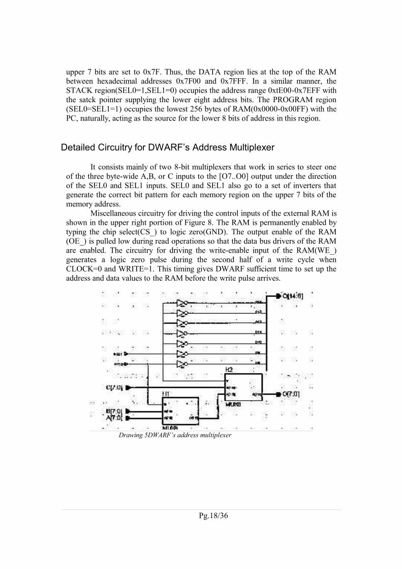
The I/O port circuitry is presented in Figure 10. The byte-wide output portis built eight flip-flops located in the IOBs along the periphery of the FPGA(moduleOFDEX8). Thus these flip-flops do not consume resources in the FPGA’s CLBarray. When LD_PORT=1 and a rising edge occurs on the CLOCK signal, the[OUT_PORT7..OUT_PORT0] pins will retain the value that was on the D bus atthat time. The value is always actively driven-onto the pins because the tristatebuffers at the outputs of the flip-flops have their enable signals tied to logic one(VCC).
The input side of the I/O circuitry consists of eight input signals whosevalues are loaded into flip-flops in the IOBs(IFD8) of the FPGA on every risingedge of the clock. The value clocked into the flip-flops is driven onto the D buswhen a logic one is applied to the DRV_D_PORT signal. WE use flip-flops becausethey synchronize the input signal transitions to the same clock that drives the rest ofDWARF. This reduces the chance that one of DWARF’s internal flip-flops willenter a metastable state due to a change on one of the inputs just asa clock edgeoccurs.
DWARF’s Interrupt-Handling Circuitry
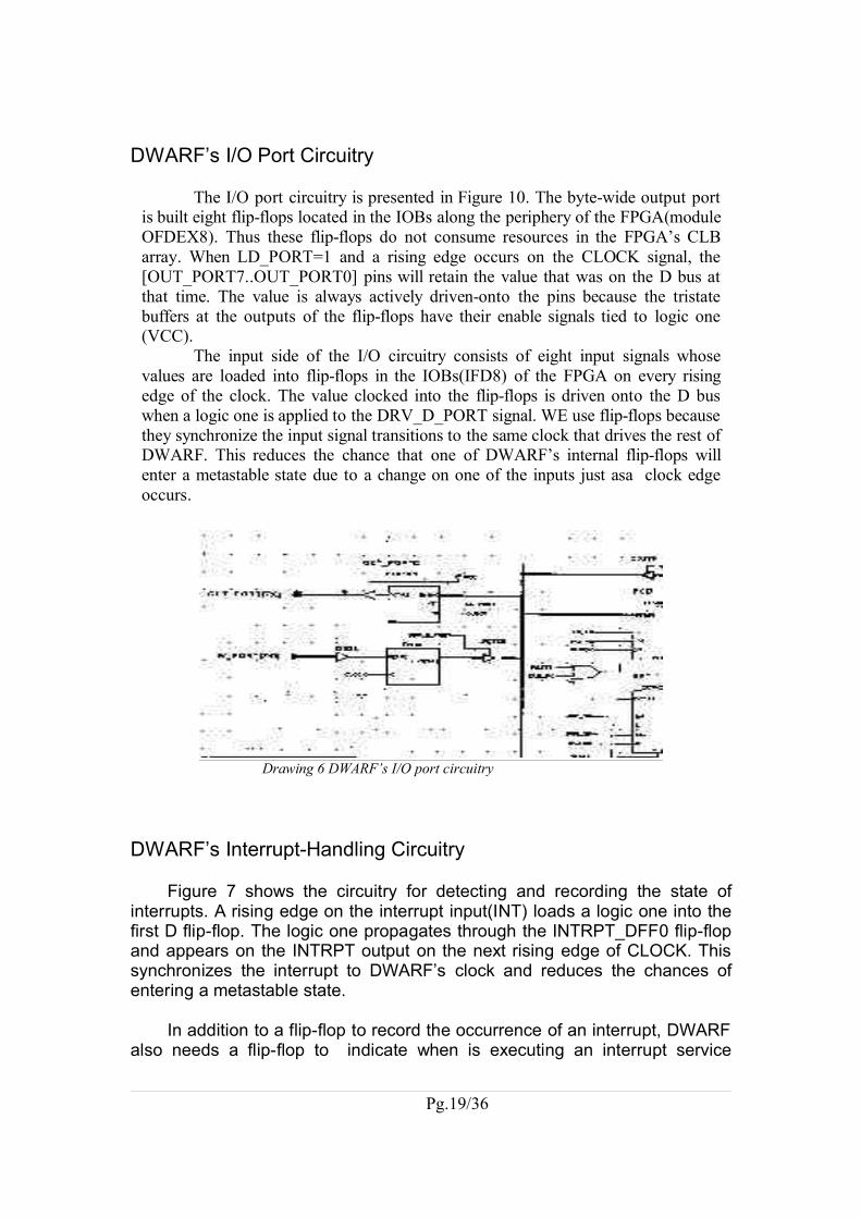
Figure 7 shows the circuitry for detecting and recording the state ofinterrupts. A rising edge on the interrupt input(INT) loads a logic one into thefirst D flip-flop. The logic one propagates through the INTRPT_DFF0 flip-flopand appears on the INTRPT output on the next rising edge of CLOCK. Thissynchronizes the interrupt to DWARF’s clock and reduces the chances ofentering a metastable state.
In addition to a flip-flop to record the occurrence of an interrupt, DWARFalso needs a flip-flop to indicate when is executing an interrupt service
Pg.19/36
Drawing 6 DWARF’s I/O port circuitry
routine. The IFLAGO flip-flop serves this purpose. IFLAGO is set to a logicone state when SET_IFLAG=1.The IFLAG output from the flip-flop is used toswitch to the alternate set of eight registers in the DWRF_REG module. Also,both IFLAG and INTRPT are inputs to the instruction decoder. If INTRPT=1and IFLAG=0, the instruction decoder will alter the flow of instructions byinitiating the interrupt service routine. But if INTRPT=1 and IFLAG=1,DWARF will ignore the pending intrrupt, because it is already processing aninterrupt.
The interrupt flip-flops are cleared when the CLR_INTRPT andCLR_IFLAG are high. The CLR_INTRPT signal is asserted to clear theINTERPT flag when the interrupt routine is entered. This minimizes theamount of time that passes before the circuitry can detect another interrupt.The CLR_IFLAG signal, however, is asserted as the processor is leaving theISR. The RESET signal also clears the INTRPT and IFLAG flip-flops so thatDWARF does not erroneously beginprocessing an interrupt when it first startsup.
Figure 7 also shows how the clock and reset signals enter DWARF. Boththe IN_RESET and IN_CLOCK inputs enter through normal IBUF’s. But theIN_CLOCK input then passes through a primary global buffer(symbol
BUFGP). The use of such a buffer allows the clock signal to travel over aglobal net that does not suffer from the delays incurred by signals thet travelthrough the routing switches. Thus, the CLOCK signal has very low skew andclock edges will reach all the flip-flops at nearly the same instant.
Pg.20/36
Drawing 7DWARF’s Interrupt circuitry
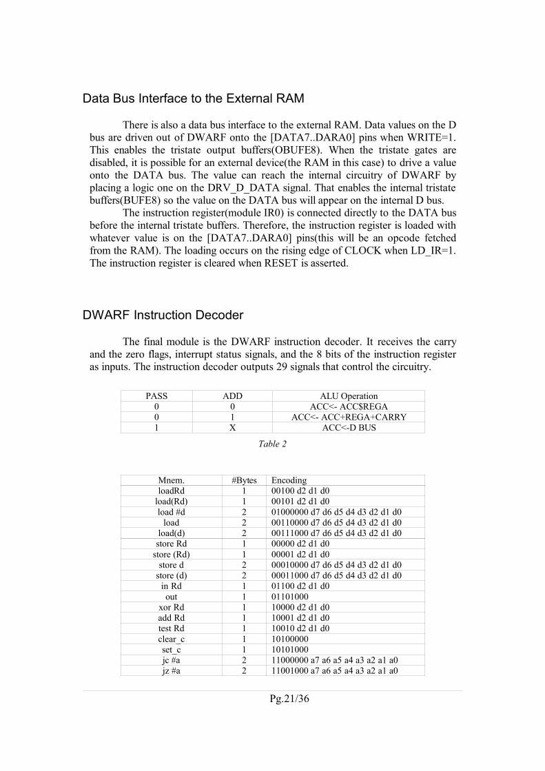
Data Bus Interface to the External RAM
There is also a data bus interface to the external RAM. Data values on the Dbus are driven out of DWARF onto the [DATA7..DARA0] pins when WRITE=1.This enables the tristate output buffers(OBUFE8). When the tristate gates aredisabled, it is possible for an external device(the RAM in this case) to drive a valueonto the DATA bus. The value can reach the internal circuitry of DWARF byplacing a logic one on the DRV_D_DATA signal. That enables the internal tristatebuffers(BUFE8) so the value on the DATA bus will appear on the internal D bus.
The instruction register(module IR0) is connected directly to the DATA busbefore the internal tristate buffers. Therefore, the instruction register is loaded withwhatever value is on the [DATA7..DARA0] pins(this will be an opcode fetchedfrom the RAM). The loading occurs on the rising edge of CLOCK when LD_IR=1.The instruction register is cleared when RESET is asserted.
DWARF Instruction Decoder
The final module is the DWARF instruction decoder. It receives the carryand the zero flags, interrupt status signals, and the 8 bits of the instruction registeras inputs. The instruction decoder outputs 29 signals that control the circuitry.
PASS ADD ALU Operation0 0 ACC<- ACC$REGA0 1 ACC<- ACC+REGA+CARRY1 X ACC<-D BUS
Table 2
Mnem. #Bytes EncodingloadRd 1 00100 d2 d1 d0
load(Rd) 1 00101 d2 d1 d0load #d 2 01000000 d7 d6 d5 d4 d3 d2 d1 d0
load 2 00110000 d7 d6 d5 d4 d3 d2 d1 d0load(d) 2 00111000 d7 d6 d5 d4 d3 d2 d1 d0store Rd 1 00000 d2 d1 d0
store (Rd) 1 00001 d2 d1 d0store d 2 00010000 d7 d6 d5 d4 d3 d2 d1 d0
store (d) 2 00011000 d7 d6 d5 d4 d3 d2 d1 d0in Rd 1 01100 d2 d1 d0out 1 01101000
xor Rd 1 10000 d2 d1 d0add Rd 1 10001 d2 d1 d0test Rd 1 10010 d2 d1 d0clear_c 1 10100000 set_c 1 10101000 jc #a 2 11000000 a7 a6 a5 a4 a3 a2 a1 a0jz #a 2 11001000 a7 a6 a5 a4 a3 a2 a1 a0
Pg.21/36
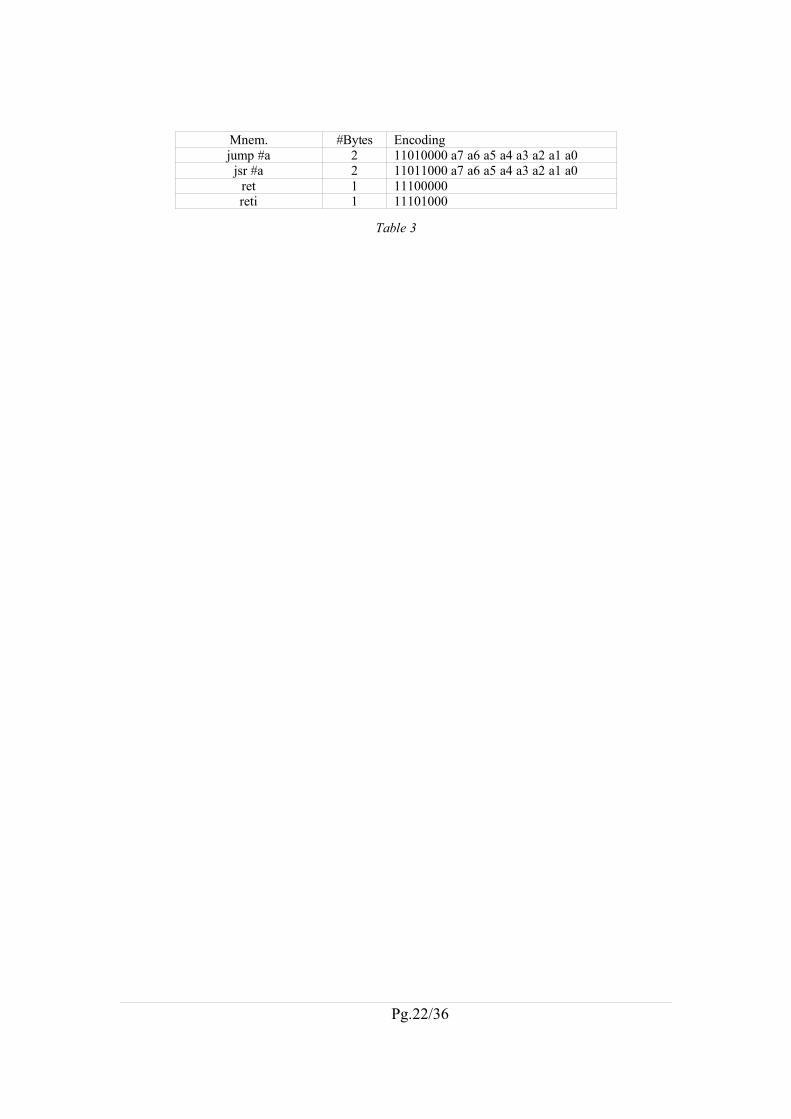
Mnem. #Bytes Encodingjump #a 2 11010000 a7 a6 a5 a4 a3 a2 a1 a0
jsr #a 2 11011000 a7 a6 a5 a4 a3 a2 a1 a0ret 1 11100000reti 1 11101000
Table 3
Pg.22/36
Part I (cont)
DWARF BASIC ARCHITECTURE.........................................................13STACK POINTER (SP)....................................................................... 14REGISTER SET(R0-R7)......................................................................14I/O PORT(IOP) ................................................................................... 14ADDRESS SELECTOR....................................................................... 14INTERRUPT DETECTOR.................................................................. 15D BUS...................................................................................................15DWARF’S REGISTER SET AND ALU............................................. 15DWARF’S ARITHMETIC CIRCUITRY............................................ 16DWARF’S CARRY FLAG...................................................................16DWARF’S PROGRAM COUNTER, STACK POINTER, ADDRESSSELECTOR, AND RAM CONTROL CIRCUITRY........................... 17DETAILED CIRCUITRY FOR DWARF’S ADDRESSMULTIPLEXER...................................................................................18DWARF’S I/O PORT CIRCUITRY.................................................... 19DWARF’S INTERRUPT-HANDLING CIRCUITRY.........................20DATA BUS INTERFACE TO THE EXTERNAL RAM.................... 21DWARF INSTRUCTION DECODER.................................................22
Pg.23/36
Part II
Source Code
All the programming was done using Icarus Verilog v.0.7
Requirements
To compile the software, make sure you have Icarus Verilog Path set andrun:
iverilog *.v -o dwarf.outTo run the program, use:
vvp dwarf.out
Source Code
Dwarf's ALU (alu.v)ALU is the Arithmeticand Logical unit of the DWARF microprocessor.
Next, is the listed code, written in verilog.
Source Listing/* * Module: ALU * * Description: * Dwarf Arithmetical Logical * Unit (ALU) * * Inputs: * //Control * clk - Clock * rst - Reset * set_cry - see Carry0 Module * alu_cry - see Carry0 Module * ld_cry - see Carry0 Module * ld_acc - * ld_z - * add - pass = 0; add = 0; Acc<-Acc$REGA * pass = 0; add = 1; ACC<-ACC+REGA+CARRY * pass - pass = 1; add = x; ACC<-D Bus * //Data * A[7:0] - D_BUS * R[7:0] - Register * * Outputs: * //Control * carry - Carry0 Module result
Pg.24/36
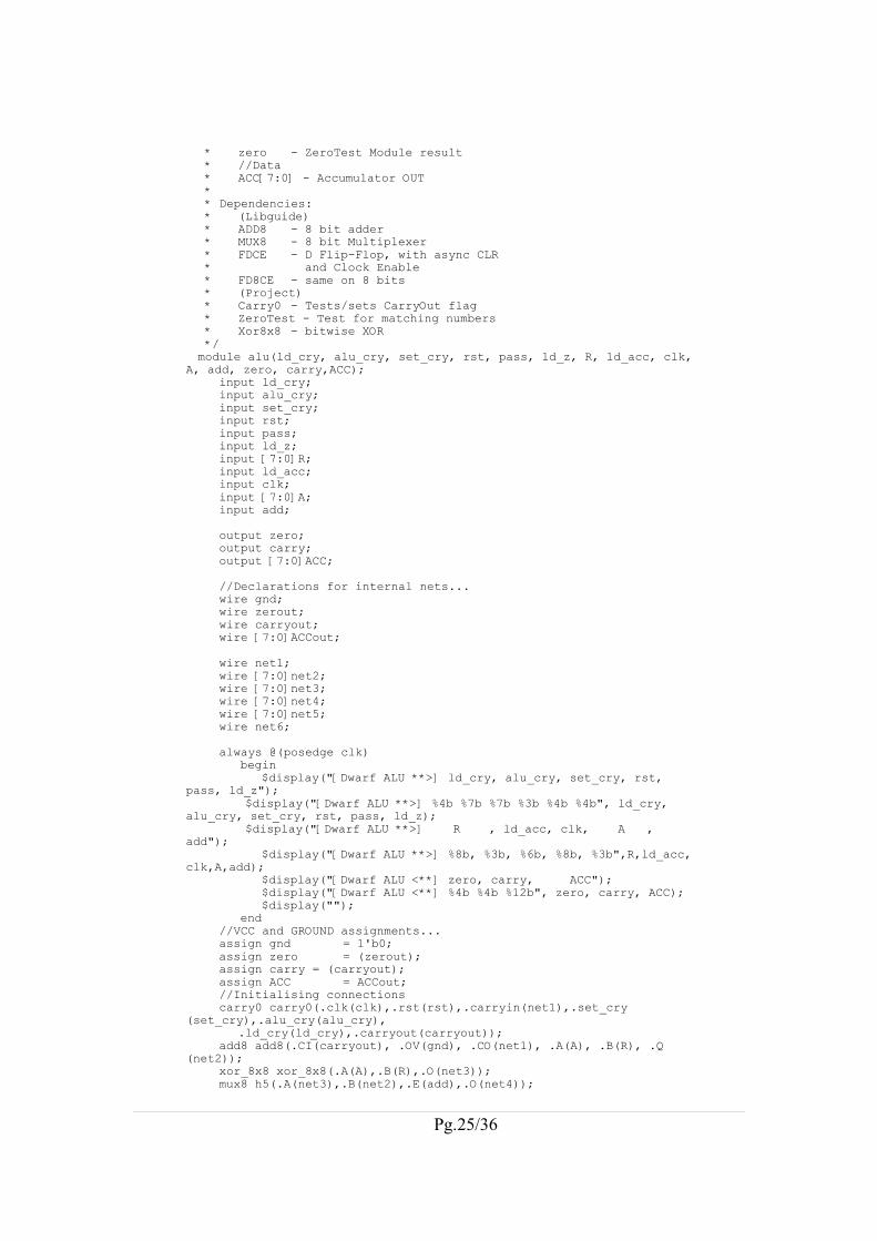
* zero - ZeroTest Module result * //Data * ACC[7:0] - Accumulator OUT * * Dependencies: * (Libguide) * ADD8 - 8 bit adder * MUX8 - 8 bit Multiplexer * FDCE - D Flip-Flop, with async CLR * and Clock Enable * FD8CE - same on 8 bits * (Project) * Carry0 - Tests/sets CarryOut flag * ZeroTest - Test for matching numbers * Xor8x8 - bitwise XOR */module alu(ld_cry, alu_cry, set_cry, rst, pass, ld_z, R, ld_acc, clk,
A, add, zero, carry,ACC); input ld_cry; input alu_cry; input set_cry; input rst; input pass; input ld_z; input [7:0]R; input ld_acc; input clk; input [7:0]A; input add;
output zero; output carry; output [7:0]ACC;
//Declarations for internal nets... wire gnd; wire zerout; wire carryout; wire [7:0]ACCout;
wire net1; wire [7:0]net2; wire [7:0]net3; wire [7:0]net4; wire [7:0]net5; wire net6;
always @(posedge clk) begin $display("[Dwarf ALU **>] ld_cry, alu_cry, set_cry, rst,
pass, ld_z"); $display("[Dwarf ALU **>] %4b %7b %7b %3b %4b %4b", ld_cry,
alu_cry, set_cry, rst, pass, ld_z); $display("[Dwarf ALU **>] R , ld_acc, clk, A ,
add"); $display("[Dwarf ALU **>] %8b, %3b, %6b, %8b, %3b",R,ld_acc,
clk,A,add); $display("[Dwarf ALU <**] zero, carry, ACC"); $display("[Dwarf ALU <**] %4b %4b %12b", zero, carry, ACC); $display(""); end //VCC and GROUND assignments... assign gnd = 1'b0; assign zero = (zerout); assign carry = (carryout); assign ACC = ACCout; //Initialising connections carry0 carry0(.clk(clk),.rst(rst),.carryin(net1),.set_cry
(set_cry),.alu_cry(alu_cry),.ld_cry(ld_cry),.carryout(carryout));
add8 add8(.CI(carryout), .OV(gnd), .CO(net1), .A(A), .B(R), .Q(net2)); xor_8x8 xor_8x8(.A(A),.B(R),.O(net3)); mux8 h5(.A(net3),.B(net2),.E(add),.O(net4));
Pg.25/36
mux8 h2(.A(net4),.B(A),.E(pass),.O(net5)); zerotest h3(.A(A),.B(R),.Q(net6)); fdce zero0(.CLR(rst),.CE(ld_z),.C(clk),.D(net6),.Q(zerout)); fd8ce accum0(.CLR(rst),.CE(ld_acc),.C(clk),.D(net5),.Q(ACCout));endmodule
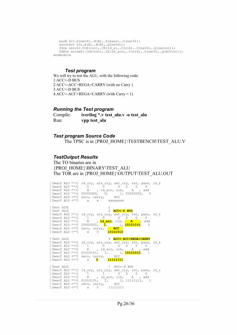
Test programWe will try to test the ALU, with the following code:1.ACC<-D BUS2.ACC<-ACC+REGA+CARRY (with no Carry )3.ACC<-D BUS4.ACC<-ACC+REGA+CARRY (with Carry = 1)
Running the Test programCompile: iverilog *.v test_alu.v -o test_aluRun: vpp test_alu
Test program Source CodeThe TPSC is in {PROJ_HOME}\TESTBENCH\TEST_ALU.V
TestOutput ResultsThe TO binaries are in {PROJ_HOME}\BINARY\TEST_ALUThe TOR are in {PROJ_HOME}\OUTPUT\TEST_ALU.OUT
[Dwarf ALU **>] ld_cry, alu_cry, set_cry, rst, pass, ld_z[Dwarf ALU **>] 0 0 0 0 0 0[Dwarf ALU **>] R , ld_acc, clk, A , add[Dwarf ALU **>] 00000000, 0, 1, 00000000, 0[Dwarf ALU <**] zero, carry, ACC[Dwarf ALU <**] x x xxxxxxxx
[Test ALU] 1[Test ALU] 2 ACC<-D BUS[Dwarf ALU **>] ld_cry, alu_cry, set_cry, rst, pass, ld_z[Dwarf ALU **>] 1 0 0 0 0 0[Dwarf ALU **>] R , ld_acc, clk, A , add[Dwarf ALU **>] 00000000, 1, 1, 10101010, 0[Dwarf ALU <**] zero, carry, ACC [Dwarf ALU <**] x 0 10101010[Test ALU] 4 ACC<-ACC+REGA+CARRY[Dwarf ALU **>] ld_cry, alu_cry, set_cry, rst, pass, ld_z[Dwarf ALU **>] 1 0 0 0 0 0[Dwarf ALU **>] R , ld_acc, clk, A , add[Dwarf ALU **>] 01010101, 1, 1, 10101010, 1[Dwarf ALU <**] zero, carry, ACC[Dwarf ALU <**] x 0 11111111[Test ALU] 7 ACC<-D BUS[Dwarf ALU **>] ld_cry, alu_cry, set_cry, rst, pass, ld_z[Dwarf ALU **>] 1 1 0 0 0 0[Dwarf ALU **>] R , ld_acc, clk, A , add[Dwarf ALU **>] 01010101, 1, 1, 11111111, 1[Dwarf ALU <**] zero, carry, ACC[Dwarf ALU <**] x 0 11111111
Pg.26/36
[Dwarf ALU **>] ld_cry, alu_cry, set_cry, rst, pass, ld_z[Dwarf ALU **>] 1 1 0 0 0 0[Dwarf ALU **>] R , ld_acc, clk, A , add[Dwarf ALU **>] 01010101, 1, 1, 11111111, 1[Dwarf ALU <**] zero, carry, ACC[Dwarf ALU <**] x 1 01010100[Test ALU] 11 ACC<-ACC+REGA+CARRY[Dwarf ALU **>] ld_cry, alu_cry, set_cry, rst, pass, ld_z[Dwarf ALU **>] 1 1 0 0 0 0[Dwarf ALU **>] R , ld_acc, clk, A , add[Dwarf ALU **>] 01010101, 1, 1, 11111111, 1[Dwarf ALU <**] zero, carry, ACC[Dwarf ALU <**] x 1 01010101[Dwarf ALU **>] ld_cry, alu_cry, set_cry, rst, pass, ld_z[Dwarf ALU **>] 1 1 0 0 0 0[Dwarf ALU **>] R , ld_acc, clk, A , add[Dwarf ALU **>] 01010101, 1, 1, 11111111, 1[Dwarf ALU <**] zero, carry, ACC[Dwarf ALU <**] x 1 01010101
[Dwarf ALU **>] ld_cry, alu_cry, set_cry, rst, pass, ld_z[Dwarf ALU **>] 1 1 0 0 0 0[Dwarf ALU **>] R , ld_acc, clk, A , add[Dwarf ALU **>] 01010101, 1, 1, 11111111, 1[Dwarf ALU <**] zero, carry, ACC [Dwarf ALU <**] x 1 01010101
TestOutput Explanations[TODO]
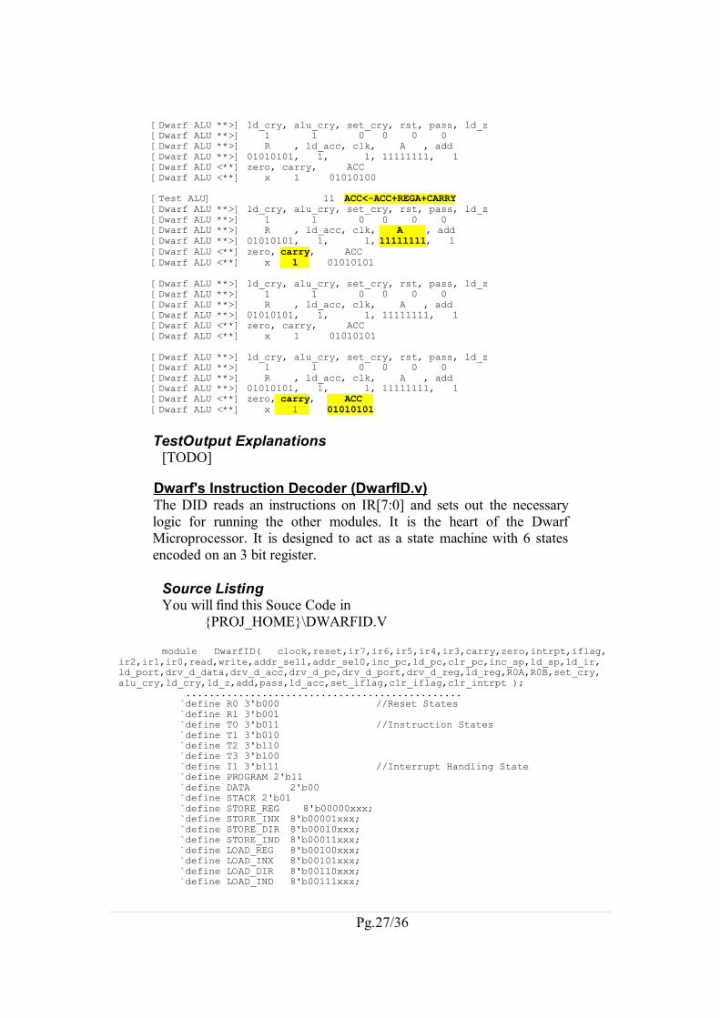
Dwarf's Instruction Decoder (DwarfID.v)The DID reads an instructions on IR[7:0] and sets out the necessarylogic for running the other modules. It is the heart of the DwarfMicroprocessor. It is designed to act as a state machine with 6 statesencoded on an 3 bit register.
Source ListingYou will find this Souce Code in
{PROJ_HOME}\DWARFID.V
module DwarfID( clock,reset,ir7,ir6,ir5,ir4,ir3,carry,zero,intrpt,iflag,ir2,ir1,ir0,read,write,addr_sel1,addr_sel0,inc_pc,ld_pc,clr_pc,inc_sp,ld_sp,ld_ir,ld_port,drv_d_data,drv_d_acc,drv_d_pc,drv_d_port,drv_d_reg,ld_reg,R0A,R0B,set_cry,alu_cry,ld_cry,ld_z,add,pass,ld_acc,set_iflag,clr_iflag,clr_intrpt );
............................................... `define R0 3'b000 //Reset States `define R1 3'b001 `define T0 3'b011 //Instruction States `define T1 3'b010 `define T2 3'b110 `define T3 3'b100 `define I1 3'b111 //Interrupt Handling State `define PROGRAM 2'b11 `define DATA 2'b00 `define STACK 2'b01 `define STORE_REG 8'b00000xxx; `define STORE_INX 8'b00001xxx; `define STORE_DIR 8'b00010xxx; `define STORE_IND 8'b00011xxx; `define LOAD_REG 8'b00100xxx; `define LOAD_INX 8'b00101xxx; `define LOAD_DIR 8'b00110xxx; `define LOAD_IND 8'b00111xxx;
Pg.27/36
`define LOAD_IMM 8'b01000xxx; `define IN_REG 8'b01100xxx; `define OUT 8'b01101xxx; `define XOR 8'b10000xxx; `define ADD 8'b10001xxx; `define TEST 8'b10010xxx; `define CLEAR_C 8'b10100xxx; `define SET_C 8'b10101xxx; `define JC 8'b11000xxx; `define JZ 8'b11001xxx; `define JUMP 8'b11010xxx; `define JSR 8'b11011xxx; `define RET 8'b11100xxx; `define RETI 8'b11101xxx;................................................ always @ (ir or CurrState) begin $display("Ma Lansez");
NextState = CurrState;case (CurrState)
`R0:begin ld_pc = 1; inc_pc = 1; inc_pc=1; NextState = `R1;end
`R1:begin ld_pc = 1; inc_pc = 1; NextState = `T0;end
`T0:begin $display("Pizdici"); if ((intrpt==1) && (iflag==0)) begin
NextState = `I1;clr_intrpt = 1;set_iflag = 1;drv_d_pc = 1;addr_sel = `STACK; write = 1;ld_sp = 1; inc_sp = 1;
end else begin
NextState = `T1;addr_sel = `PROGRAM; read = 1;drv_d_data = 1; ld_ir = 1;ld_pc = 1; inc_pc = 1;
endend`I1:begin
NextState = `T0; drv_d_acc = 1; ld_sp = 1; inc_sp = 1;
clr_pc = 1;end
...................................................`T3: begin //case(ir) if (ir[7:3]==5'b11011)
//`JSR:begin NextState = `T0; drv_d_reg=1; R0B=1; ld_pc=1;end
else if (ir[7:3]==5'b11101)
Pg.28/36
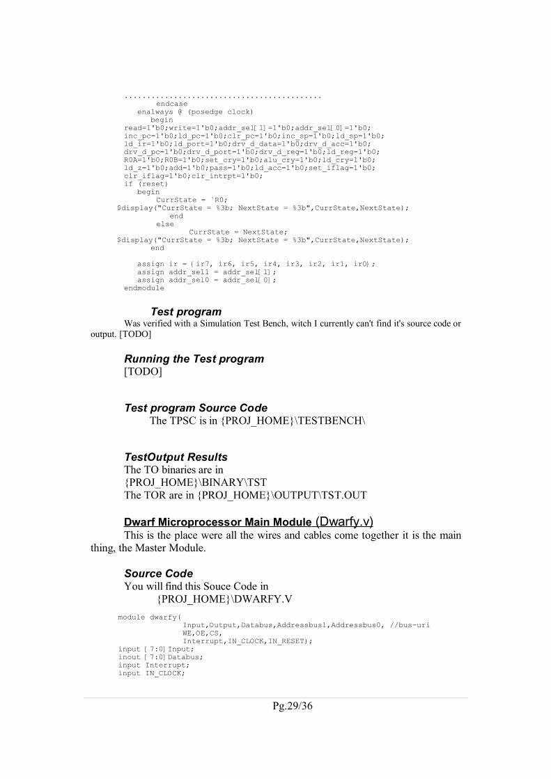
............................................endcase
enalways @ (posedge clock) beginread=1'b0;write=1'b0;addr_sel[1]=1'b0;addr_sel[0]=1'b0;inc_pc=1'b0;ld_pc=1'b0;clr_pc=1'b0;inc_sp=1'b0;ld_sp=1'b0;ld_ir=1'b0;ld_port=1'b0;drv_d_data=1'b0;drv_d_acc=1'b0;drv_d_pc=1'b0;drv_d_port=1'b0;drv_d_reg=1'b0;ld_reg=1'b0;R0A=1'b0;R0B=1'b0;set_cry=1'b0;alu_cry=1'b0;ld_cry=1'b0;ld_z=1'b0;add=1'b0;pass=1'b0;ld_acc=1'b0;set_iflag=1'b0;clr_iflag=1'b0;clr_intrpt=1'b0;if (reset) begin
CurrState = `R0;$display("CurrState = %3b; NextState = %3b",CurrState,NextState);
endelse
CurrState = NextState;$display("CurrState = %3b; NextState = %3b",CurrState,NextState); end assign ir = {ir7, ir6, ir5, ir4, ir3, ir2, ir1, ir0}; assign addr_sel1 = addr_sel[1]; assign addr_sel0 = addr_sel[0];endmodule
Test programWas verified with a Simulation Test Bench, witch I currently can't find it's source code or
output. [TODO]
Running the Test program[TODO]
Test program Source CodeThe TPSC is in {PROJ_HOME}\TESTBENCH\
TestOutput ResultsThe TO binaries are in {PROJ_HOME}\BINARY\TSTThe TOR are in {PROJ_HOME}\OUTPUT\TST.OUT
Dwarf Microprocessor Main Module (Dwarfy.v) This is the place were all the wires and cables come together it is the main
thing, the Master Module.
Source CodeYou will find this Souce Code in
{PROJ_HOME}\DWARFY.Vmodule dwarfy(
Input,Output,Databus,Addressbus1,Addressbus0, //bus-uriWE,OE,CS,Interrupt,IN_CLOCK,IN_RESET);
input [7:0]Input;inout [7:0]Databus;input Interrupt;input IN_CLOCK;
Pg.29/36
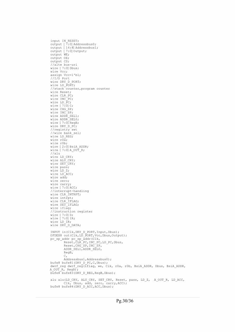
input IN_RESET;output [7:0]Addressbus0;output [14:8]Addressbus1;output [7:0]Output;output WE;output OE;output CS;//alte bus-uriwire [7:0]Dbus;wire Vcc;assign Vcc=1'b1;//I/O Portwire DRY_D_PORT;wire LD_PORT;//stack counter,program counterwire Reset;wire CLR_PC;wire INC_PC;wire LD_PC;wire [7:0]C;wire CHG_SP;wire INC_SP;wire ADDR_SEL1;wire ADDR_SEL0;wire [7:0]RegB;wire DRY_D_PC;//registry set//wire bank_sel;wire LD_REG;wire r0a;wire r0b;wire [2:0]BsiA_ADDR;wire [7:0]A_OUT_R;//aluwire LD_CRY;wire ALU_CRY;wire SET_CRY;wire pass;wire LD_Z;wire LD_ACC;wire add;wire zero;wire carry;wire [7:0]ACC;//interrupt-handlingwire CLR_INTRPT;wire intrpt;wire CLR_IFLAG;wire SET_IFLAG;wire iflag;//instruction registerwire [7:0]D;wire [7:0]IR;wire LD_IR;wire DRY_D_DATA;
INPUT in(Clk,DRY_D_PORT,Input,Dbus);OFDEX8 out(Clk,LD_PORT,Vcc,Dbus,Output);pc_sp_addr pc_sp_addr(Clk,
Reset,CLR_PC,INC_PC,LD_PC,Dbus,Reset,CHG_SP,INC_SP,ADDR_SEL1,ADDR_SEL0,RegB,C,Addressbus1,Addressbus0);
bufe8 bufe81(DRY_D_PC,C,Dbus);dwrf_reg dwrf_reg(iflag, we, Clk, r0a, r0b, BsiA_ADDR, Dbus, BsiA_ADDR,A_OUT_R, RegB);bufe8 bufe83(DRY_D_REG,RegB,Dbus);
alu alu(LD_CRY, ALU_CRY, SET_CRY, Reset, pass, LD_Z, A_OUT_R, LD_ACC, Clk, Dbus, add, zero, carry,ACC);
bufe8 bufe84(DRY_D_ACC,ACC,Dbus);
Pg.30/36
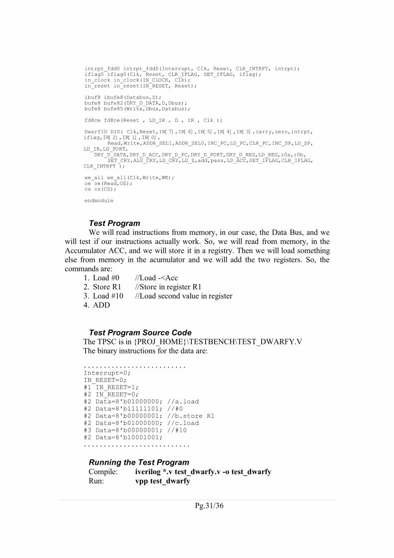
intrpt_fdd0 intrpt_fdd0(Interrupt, Clk, Reset, CLR_INTRPT, intrpt);iflag0 iflag0(Clk, Reset, CLR_IFLAG, SET_IFLAG, iflag);in_clock in_clock(IN_CLOCK, Clk);in_reset in_reset(IN_RESET, Reset);
ibuf8 ibufe8(Databus,D);bufe8 bufe82(DRY_D_DATA,D,Dbus);bufe8 bufe85(Write,Dbus,Databus);
fd8ce fd8ce(Reset , LD_IR , D , IR , Clk ); DwarfID DID( Clk,Reset,IR[7],IR[6],IR[5],IR[4],IR[3],carry,zero,intrpt,iflag,IR[2],IR[1],IR[0], Read,Write,ADDR_SEL1,ADDR_SEL0,INC_PC,LD_PC,CLR_PC,INC_SP,LD_SP,LD_IR,LD_PORT, DRY_D_DATA,DRY_D_ACC,DRY_D_PC,DRY_D_PORT,DRY_D_REG,LD_REG,r0a,r0b, SET_CRY,ALU_CRY,LD_CRY,LD_Z,add,pass,LD_ACC,SET_IFLAG,CLR_IFLAG,CLR_INTRPT );we_all we_all(Clk,Write,WE);oe oe(Read,OE);cs cs(CS);
endmodule
Test ProgramWe will read instructions from memory, in our case, the Data Bus, and we
will test if our instructions actually work. So, we will read from memory, in theAccumulator ACC, and we will store it in a registry. Then we will load somethingelse from memory in the acumulator and we will add the two registers. So, thecommands are:
1. Load #0 //Load -<Acc2. Store R1 //Store in register R13. Load #10 //Load second value in register4. ADD
Test Program Source CodeThe TPSC is in {PROJ_HOME}\TESTBENCH\TEST_DWARFY.VThe binary instructions for the data are:
..........................Interrupt=0;IN_RESET=0;#1 IN_RESET=1;#2 IN_RESET=0;#2 Data=8'b01000000; //a.load #2 Data=8'b11111101; //#0#2 Data=8'b00000001; //b.store R1#2 Data=8'b01000000; //c.load #3 Data=8'b00000001; //#10#2 Data=8'b10001001;...........................
Running the Test ProgramCompile: iverilog *.v test_dwarfy.v -o test_dwarfyRun: vpp test_dwarfy
Pg.31/36
Test Program Output{PROJ_HOME}\BINARY\OUTPUT_PR2.TXT
Test Output Explanation[TODO]
Program Example
We will use a test program to verify our mircopocessor. The test programmust calculate the Cyclic Redundancy Check of a chunk of data.
Source Codeon the webSource Code Explanationson the webTest Resultson the web
Pg.32/36
Part II
SOURCE CODE....................................................................................... 24REQUIREMENTS............................................................................... 24SOURCE CODE...................................................................................24
Dwarf's ALU (alu.v)............................................................................................24Source Listing.................................................................................................24Test program.................................................................................................. 26Running the Test program.............................................................................. 26Test program Source Code.............................................................................26TestOutput Results......................................................................................... 26TestOutput Explanations................................................................................ 27
Dwarf's Instruction Decoder (DwarfID.v).......................................................... 27Source Listing.................................................................................................27Test program.................................................................................................. 29Running the Test program.............................................................................. 29Test program Source Code.............................................................................29TestOutput Results......................................................................................... 29
Dwarf Microprocessor Main Module (Dwarfy.v)............................................... 29Source Code................................................................................................... 29Test Program.................................................................................................. 31Test Program Source Code............................................................................ 31Running the Test Program..............................................................................31Test Program Output......................................................................................32Test Output Explanation.................................................................................32PROGRAM EXAMPLE....................................................................... 32
Source Code........................................................................................................32Source Code Explanations.................................................................................. 32Test Results......................................................................................................... 32
Pg.33/36
APPENDIX
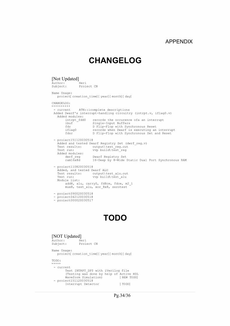
CHANGELOG
[Not Updated]Author: HeriSubject: Proiect CN
Name Usage: proiect[creation_time][year][month][day]
CHANGELOG:********** - current ATN::icomplete descriptions Added Dwarf's interrupt-handling circuitry (intrpt.v, iflag0.v) Added modules: intrpt_fdd0 records the occurence ofa an interrupt
ibuf Single-Input Buffersfdr D Flip-Flop with Synchronous Resetiflag0 records when Dwarf is executing an interruptfdsr D Flip-Flop with Synchronous Set and Reset
- proiect151120030518 Added and tested Dwarf Registry Set (dwrf_reg.v) Test results: output\test_reg.out Test run: vvp build\test_reg Added modules:
dwrf_reg Dwarf Registry Setram16x8d 16-Deep by 8-Wide Static Dual Port Synchronous RAM
- proiect110820030518 Added, and tested Dwarf ALU Test results: output\test_alu.out Test run: vvp build\test_alu Module list:
add8, alu, carry0, fd8ce, fdce, m2_1mux8, test_alu, xor_8x8, zerotest
- proiect090020030518 - proiect042120030518 - proiect000020030517
TODO
[NOT Updated]Author: HeriSubject: Proiect CNName Usage: proiect[creation_time][year][month][day]
TODO:***** - current
Test INTRPT_DF0 with iVerilog file(Testing was done by help of Active HDLWaveform Simulation) [NEW TODO]
- proiect151120030518Interrupt Detector [TODO]
Pg.34/36
Test Instruction Decoder [TODO] RegisterSet [Finished]
- proiect110820030518RegisterSet, [TODO] Interrupt Detector, [TODO] Test Instruction Decoder [TODO]
- proiect090020030518 - proiect042120030518
– proiect000020030517
Instructions Set
The dwarf's instruction set usage
Mnem. #Bytes EncodingloadRd 1 00100 d2 d1 d0
load(Rd) 1 00101 d2 d1 d0load #d 2 01000000 d7 d6 d5 d4 d3 d2 d1 d0
load 2 00110000 d7 d6 d5 d4 d3 d2 d1 d0load(d) 2 00111000 d7 d6 d5 d4 d3 d2 d1 d0store Rd 1 00000 d2 d1 d0
store (Rd) 1 00001 d2 d1 d0store d 2 00010000 d7 d6 d5 d4 d3 d2 d1 d0
store (d) 2 00011000 d7 d6 d5 d4 d3 d2 d1 d0in Rd 1 01100 d2 d1 d0out 1 01101000
xor Rd 1 10000 d2 d1 d0add Rd 1 10001 d2 d1 d0test Rd 1 10010 d2 d1 d0clear_c 1 10100000 set_c 1 10101000 jc #a 2 11000000 a7 a6 a5 a4 a3 a2 a1 a0jz #a 2 11001000 a7 a6 a5 a4 a3 a2 a1 a0
jump #a 2 11010000 a7 a6 a5 a4 a3 a2 a1 a0jsr #a 2 11011000 a7 a6 a5 a4 a3 a2 a1 a0
ret 1 11100000reti 1 11101000
Table 4
Pg.35/36

Bibliography
LIBGUIDE: , Libraries Guide - Xilinx Unified Libraries,
[TODO]
Pg.36/36